

636
6 Reverse Engineering of Microcircuits
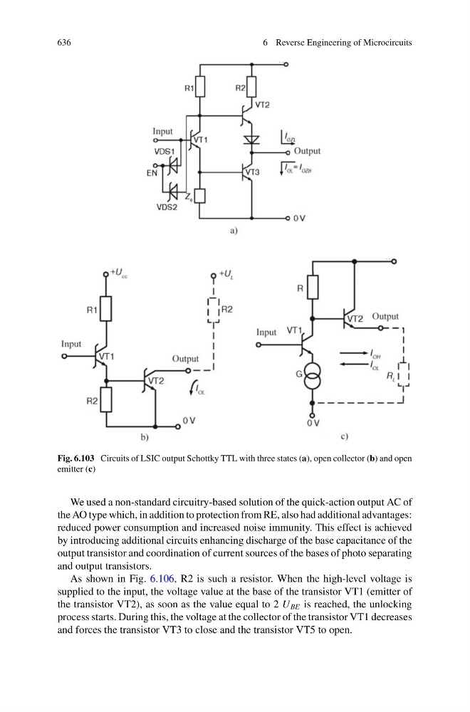
Fig. 6.103 Circuits of LSIC output Schottky TTL with three states (a), open collector (b) and open
emitter (c)
We used a non-standard circuitry-based solution of the quick-action output AC of
the AO type which, in addition to protection from RE, also had additional advantages:
reduced power consumption and increased noise immunity. This effect is achieved
by introducing additional circuits enhancing discharge of the base capacitance of the
output transistor and coordination of current sources of the bases of photo separating
and output transistors.
As shown in Fig. 6.106, R2 is such a resistor. When the high-level voltage is
supplied to the input, the voltage value at the base of the transistor VT1 (emitter of
the transistor VT2), as soon as the value equal to 2 U BE is reached, the unlocking
process starts. During this, the voltage at the collector of the transistor VT1 decreases
and forces the transistor VT3 to close and the transistor VT5 to open.