

6.8 Practical Examples of Implementation …
635
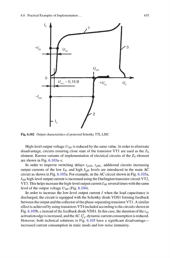
Fig. 6.102 Output characteristics of protected Schottky TTL LSIC
High-level output voltage U 0H is reduced by the same value. In order to eliminate
disadvantage, circuits ensuring close state of the transistor VT1 are used as the Z 0
element. Known variants of implementation of electrical circuits of the Z 0 element
are shown in Fig. 6.103a–c.
In order to improve switching delays t pLH , t pHL , additional circuits increasing
output currents of the low I 0L and high I QH levels are introduced in the main AC
circuit as shown in Fig. 6.105a. For example, in the AC circuit shown in Fig. 6.105a,
I 0H high-level output current is increased using the Darlington transistor circuit VT2,
VT3. This helps increase the high-level output current I 0H several times with the same
level of the output voltage U 0H (Fig. 6.104).
In order to increase the low-level output current I when the load capacitance is
discharged, the circuit is equipped with the Schottky diode VDS1 forming feedback
between the output and the collector of the phase-separating transistor VT1. A similar
effect is achieved by using transistors VT4 included according to the circuits shown in
Fig. 6.105b, c instead of the feedback diode VDS1. In this case, the duration of the t hl
activation edge is increased, and the AC I
g
CC dynamic current consumption is reduced.
However, both technical solutions in Fig. 6.105 have a significant disadvantage—
increased current consumption in static mode and low noise immunity.