

606
6 Reverse Engineering of Microcircuits
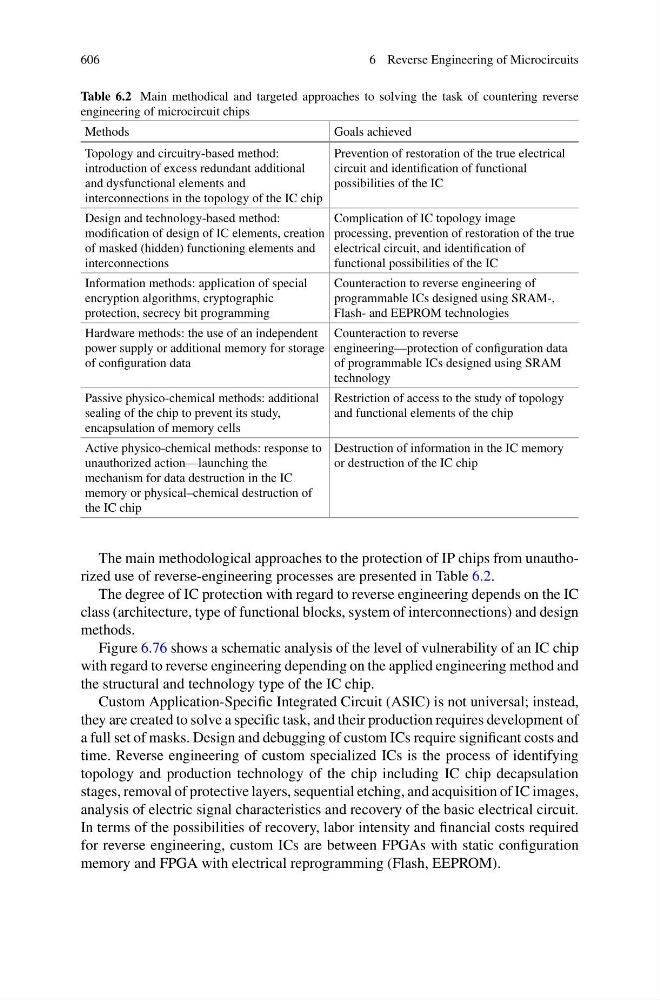
Table 6.2 Main methodical and targeted approaches to solving the task of countering reverse
engineering of microcircuit chips
Methods
Goals achieved
Topology and circuitry-based method:
introduction of excess redundant additional
and dysfunctional elements and
interconnections in the topology of the IC chip
Prevention of restoration of the true electrical
circuit and identification of functional
possibilities of the IC
Design and technology-based method:
modification of design of IC elements, creation
of masked (hidden) functioning elements and
interconnections
Complication of IC topology image
processing, prevention of restoration of the true
electrical circuit, and identification of
functional possibilities of the IC
Information methods: application of special
encryption algorithms, cryptographic
protection, secrecy bit programming
Counteraction to reverse engineering of
programmable ICs designed using SRAM-,
Flash- and EEPROM technologies
Hardware methods: the use of an independent
power supply or additional memory for storage
of configuration data
Counteraction to reverse
engineering—protection of configuration data
of programmable ICs designed using SRAM
technology
Passive physico-chemical methods: additional
sealing of the chip to prevent its study,
encapsulation of memory cells
Restriction of access to the study of topology
and functional elements of the chip
Active physico-chemical methods: response to
unauthorized action—launching the
mechanism for data destruction in the IC
memory or physical–chemical destruction of
the IC chip
Destruction of information in the IC memory
or destruction of the IC chip
The main methodological approaches to the protection of IP chips from unauthorized use of reverse-engineering processes are presented in Table 6.2.
The degree of IC protection with regard to reverse engineering depends on the IC
class (architecture, type of functional blocks, system of interconnections) and design
methods.
Figure 6.76 shows a schematic analysis of the level of vulnerability of an IC chip
with regard to reverse engineering depending on the applied engineering method and
the structural and technology type of the IC chip.
Custom Application-Specific Integrated Circuit (ASIC) is not universal; instead,
they are created to solve a specific task, and their production requires development of
a full set of masks. Design and debugging of custom ICs require significant costs and
time. Reverse engineering of custom specialized ICs is the process of identifying
topology and production technology of the chip including IC chip decapsulation
stages, removal of protective layers, sequential etching, and acquisition of IC images,
analysis of electric signal characteristics and recovery of the basic electrical circuit.
In terms of the possibilities of recovery, labor intensity and financial costs required
for reverse engineering, custom ICs are between FPGAs with static configuration
memory and FPGA with electrical reprogramming (Flash, EEPROM).
6 Reverse Engineering of Microcircuits
Table 6.2 Main methodical and targeted approaches to solving the task of countering reverse
engineering of microcircuit chips
Methods
Goals achieved
Topology and circuitry-based method:
introduction of excess redundant additional
and dysfunctional elements and
interconnections in the topology of the IC chip
Prevention of restoration of the true electrical
circuit and identification of functional
possibilities of the IC
Design and technology-based method:
modification of design of IC elements, creation
of masked (hidden) functioning elements and
interconnections
Complication of IC topology image
processing, prevention of restoration of the true
electrical circuit, and identification of
functional possibilities of the IC
Information methods: application of special
encryption algorithms, cryptographic
protection, secrecy bit programming
Counteraction to reverse engineering of
programmable ICs designed using SRAM-,
Flash- and EEPROM technologies
Hardware methods: the use of an independent
power supply or additional memory for storage
of configuration data
Counteraction to reverse
engineering—protection of configuration data
of programmable ICs designed using SRAM
technology
Passive physico-chemical methods: additional
sealing of the chip to prevent its study,
encapsulation of memory cells
Restriction of access to the study of topology
and functional elements of the chip
Active physico-chemical methods: response to
unauthorized action—launching the
mechanism for data destruction in the IC
memory or physical–chemical destruction of
the IC chip
Destruction of information in the IC memory
or destruction of the IC chip
The main methodological approaches to the protection of IP chips from unauthorized use of reverse-engineering processes are presented in Table 6.2.
The degree of IC protection with regard to reverse engineering depends on the IC
class (architecture, type of functional blocks, system of interconnections) and design
methods.
Figure 6.76 shows a schematic analysis of the level of vulnerability of an IC chip
with regard to reverse engineering depending on the applied engineering method and
the structural and technology type of the IC chip.
Custom Application-Specific Integrated Circuit (ASIC) is not universal; instead,
they are created to solve a specific task, and their production requires development of
a full set of masks. Design and debugging of custom ICs require significant costs and
time. Reverse engineering of custom specialized ICs is the process of identifying
topology and production technology of the chip including IC chip decapsulation
stages, removal of protective layers, sequential etching, and acquisition of IC images,
analysis of electric signal characteristics and recovery of the basic electrical circuit.
In terms of the possibilities of recovery, labor intensity and financial costs required
for reverse engineering, custom ICs are between FPGAs with static configuration
memory and FPGA with electrical reprogramming (Flash, EEPROM).