

604
6 Reverse Engineering of Microcircuits
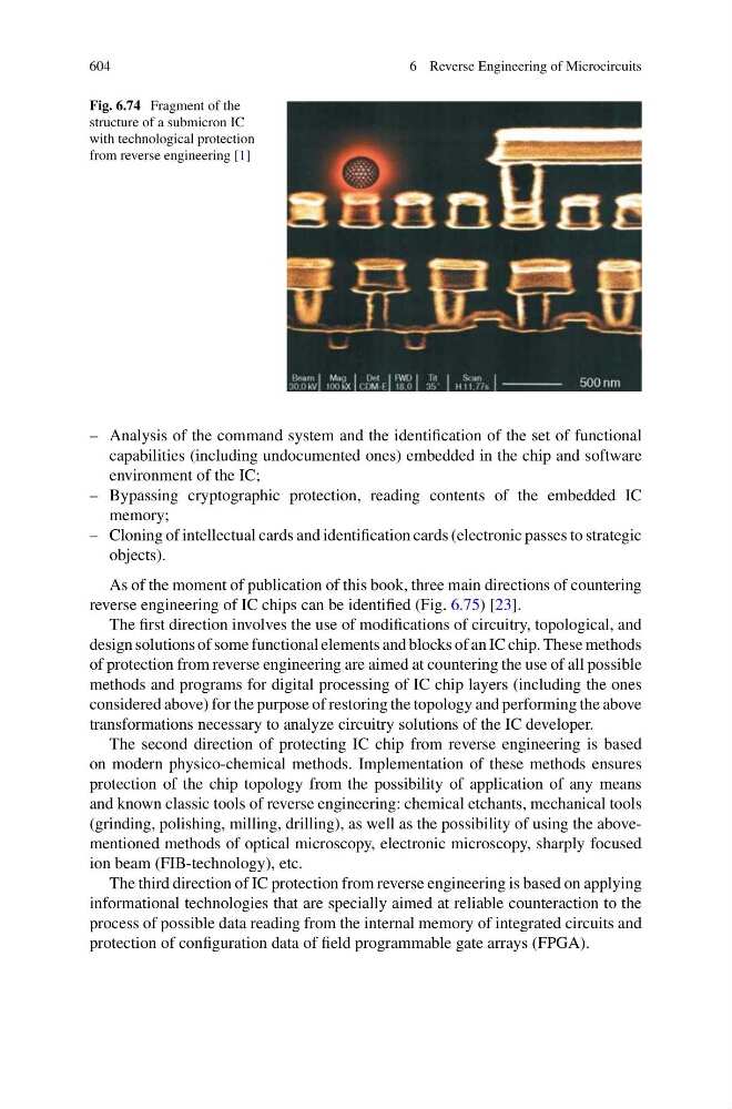
Fig. 6.74 Fragment of the
structure of a submicron IC
with technological protection
from reverse engineering [1]
– Analysis of the command system and the identification of the set of functional
capabilities (including undocumented ones) embedded in the chip and software
environment of the IC;
– Bypassing cryptographic protection, reading contents of the embedded IC
memory;
– Cloning of intellectual cards and identification cards (electronic passes to strategic
objects).
As of the moment of publication of this book, three main directions of countering
reverse engineering of IC chips can be identified (Fig. 6.75) [23].
The first direction involves the use of modifications of circuitry, topological, and
design solutions of some functional elements and blocks of an IC chip. These methods
of protection from reverse engineering are aimed at countering the use of all possible
methods and programs for digital processing of IC chip layers (including the ones
considered above) for the purpose of restoring the topology and performing the above
transformations necessary to analyze circuitry solutions of the IC developer.
The second direction of protecting IC chip from reverse engineering is based
on modern physico-chemical methods. Implementation of these methods ensures
protection of the chip topology from the possibility of application of any means
and known classic tools of reverse engineering: chemical etchants, mechanical tools
(grinding, polishing, milling, drilling), as well as the possibility of using the abovementioned methods of optical microscopy, electronic microscopy, sharply focused
ion beam (FIB-technology), etc.
The third direction of IC protection from reverse engineering is based on applying
informational technologies that are specially aimed at reliable counteraction to the
process of possible data reading from the internal memory of integrated circuits and
protection of configuration data of field programmable gate arrays (FPGA).
6 Reverse Engineering of Microcircuits
Fig. 6.74 Fragment of the
structure of a submicron IC
with technological protection
from reverse engineering [1]
– Analysis of the command system and the identification of the set of functional
capabilities (including undocumented ones) embedded in the chip and software
environment of the IC;
– Bypassing cryptographic protection, reading contents of the embedded IC
memory;
– Cloning of intellectual cards and identification cards (electronic passes to strategic
objects).
As of the moment of publication of this book, three main directions of countering
reverse engineering of IC chips can be identified (Fig. 6.75) [23].
The first direction involves the use of modifications of circuitry, topological, and
design solutions of some functional elements and blocks of an IC chip. These methods
of protection from reverse engineering are aimed at countering the use of all possible
methods and programs for digital processing of IC chip layers (including the ones
considered above) for the purpose of restoring the topology and performing the above
transformations necessary to analyze circuitry solutions of the IC developer.
The second direction of protecting IC chip from reverse engineering is based
on modern physico-chemical methods. Implementation of these methods ensures
protection of the chip topology from the possibility of application of any means
and known classic tools of reverse engineering: chemical etchants, mechanical tools
(grinding, polishing, milling, drilling), as well as the possibility of using the abovementioned methods of optical microscopy, electronic microscopy, sharply focused
ion beam (FIB-technology), etc.
The third direction of IC protection from reverse engineering is based on applying
informational technologies that are specially aimed at reliable counteraction to the
process of possible data reading from the internal memory of integrated circuits and
protection of configuration data of field programmable gate arrays (FPGA).