

6.3 Basics of Reverse-Engineering Art
545
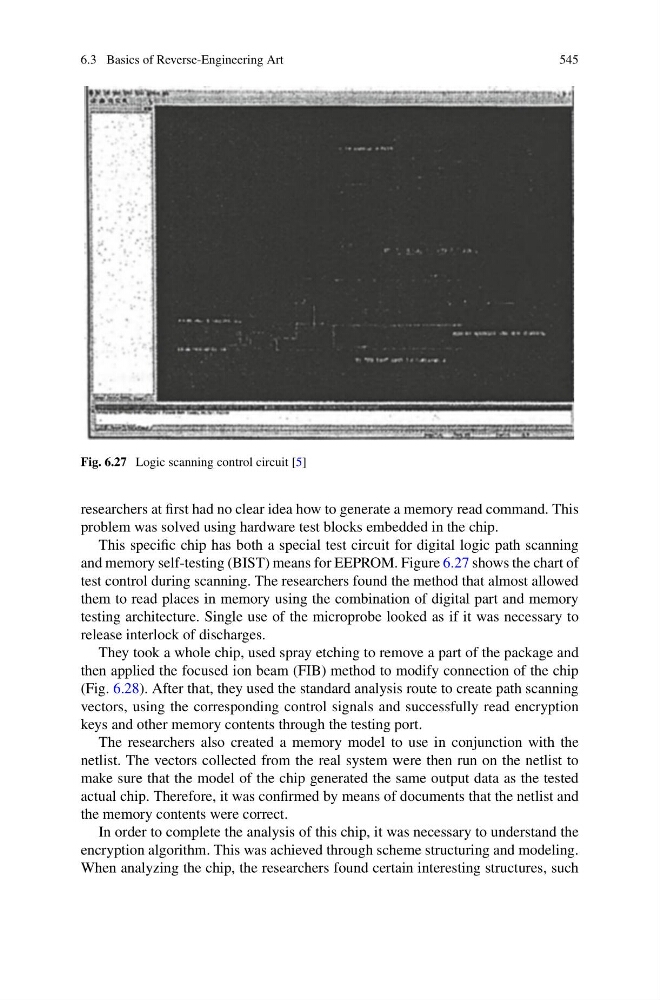
Fig. 6.27 Logic scanning control circuit [5]
researchers at first had no clear idea how to generate a memory read command. This
problem was solved using hardware test blocks embedded in the chip.
This specific chip has both a special test circuit for digital logic path scanning
and memory self-testing (BIST) means for EEPROM. Figure 6.27 shows the chart of
test control during scanning. The researchers found the method that almost allowed
them to read places in memory using the combination of digital part and memory
testing architecture. Single use of the microprobe looked as if it was necessary to
release interlock of discharges.
They took a whole chip, used spray etching to remove a part of the package and
then applied the focused ion beam (FIB) method to modify connection of the chip
(Fig. 6.28). After that, they used the standard analysis route to create path scanning
vectors, using the corresponding control signals and successfully read encryption
keys and other memory contents through the testing port.
The researchers also created a memory model to use in conjunction with the
netlist. The vectors collected from the real system were then run on the netlist to
make sure that the model of the chip generated the same output data as the tested
actual chip. Therefore, it was confirmed by means of documents that the netlist and
the memory contents were correct.
In order to complete the analysis of this chip, it was necessary to understand the
encryption algorithm. This was achieved through scheme structuring and modeling.
When analyzing the chip, the researchers found certain interesting structures, such
545
Fig. 6.27 Logic scanning control circuit [5]
researchers at first had no clear idea how to generate a memory read command. This
problem was solved using hardware test blocks embedded in the chip.
This specific chip has both a special test circuit for digital logic path scanning
and memory self-testing (BIST) means for EEPROM. Figure 6.27 shows the chart of
test control during scanning. The researchers found the method that almost allowed
them to read places in memory using the combination of digital part and memory
testing architecture. Single use of the microprobe looked as if it was necessary to
release interlock of discharges.
They took a whole chip, used spray etching to remove a part of the package and
then applied the focused ion beam (FIB) method to modify connection of the chip
(Fig. 6.28). After that, they used the standard analysis route to create path scanning
vectors, using the corresponding control signals and successfully read encryption
keys and other memory contents through the testing port.
The researchers also created a memory model to use in conjunction with the
netlist. The vectors collected from the real system were then run on the netlist to
make sure that the model of the chip generated the same output data as the tested
actual chip. Therefore, it was confirmed by means of documents that the netlist and
the memory contents were correct.
In order to complete the analysis of this chip, it was necessary to understand the
encryption algorithm. This was achieved through scheme structuring and modeling.
When analyzing the chip, the researchers found certain interesting structures, such