

532
6 Reverse Engineering of Microcircuits
6.3.2.3 Analysis of the Device Manufacturing Process
In theory, analysis of the manufacturing process is fairly simple, since the means for
such microanalysis have been well known since certain time. Each wafer-producing
semiconductor factory has its own standard set of equipment for control of the
process and analysis of failures. A number of companies specializing in RE, including
well-known Chipworks, use their own unique lab equipment. Using the Sony DCRDVD505 video camera as an example, it is possible to carry out RE operations for
CMOS sensor of the image in this camera.
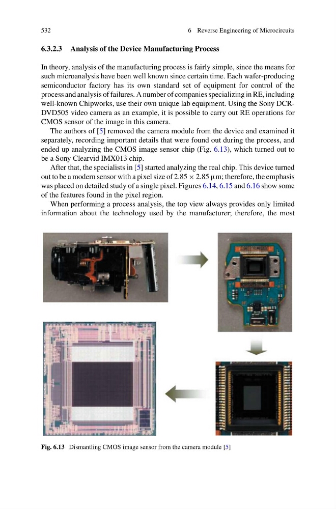
The authors of [5] removed the camera module from the device and examined it
separately, recording important details that were found out during the process, and
ended up analyzing the CMOS image sensor chip (Fig. 6.13), which turned out to
be a Sony Clearvid IMX013 chip.
After that, the specialists in [5] started analyzing the real chip. This device turned
out to be a modern sensor with a pixel size of 2.85 × 2.85 μm; therefore, the emphasis
was placed on detailed study of a single pixel. Figures 6.14, 6.15 and 6.16 show some
of the features found in the pixel region.
When performing a process analysis, the top view always provides only limited
information about the technology used by the manufacturer; therefore, the most
Fig. 6.13 Dismantling CMOS image sensor from the camera module [5]
6 Reverse Engineering of Microcircuits
6.3.2.3 Analysis of the Device Manufacturing Process
In theory, analysis of the manufacturing process is fairly simple, since the means for
such microanalysis have been well known since certain time. Each wafer-producing
semiconductor factory has its own standard set of equipment for control of the
process and analysis of failures. A number of companies specializing in RE, including
well-known Chipworks, use their own unique lab equipment. Using the Sony DCRDVD505 video camera as an example, it is possible to carry out RE operations for
CMOS sensor of the image in this camera.
The authors of [5] removed the camera module from the device and examined it
separately, recording important details that were found out during the process, and
ended up analyzing the CMOS image sensor chip (Fig. 6.13), which turned out to
be a Sony Clearvid IMX013 chip.
After that, the specialists in [5] started analyzing the real chip. This device turned
out to be a modern sensor with a pixel size of 2.85 × 2.85 μm; therefore, the emphasis
was placed on detailed study of a single pixel. Figures 6.14, 6.15 and 6.16 show some
of the features found in the pixel region.
When performing a process analysis, the top view always provides only limited
information about the technology used by the manufacturer; therefore, the most
Fig. 6.13 Dismantling CMOS image sensor from the camera module [5]