

496
5 Methods of Detecting Hardware Trojans in Microcircuits
tested wafer; in this case, all of the above data for the first tested wafer are determined
manually in accordance with the instructions of the control program.
The process of identification of defects (in case with software modification—
Trojans) here is performed automatically. Monitoring of the wafer (or a part of it)
results in the defect list protocol with indication of coordinates and sizes of defects.
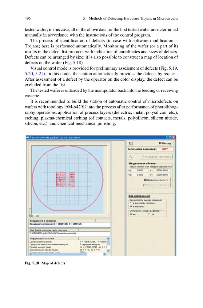
Defects can be arranged by size; it is also possible to construct a map of location of
defects on the wafer (Fig. 5.18).
Visual control mode is provided for preliminary assessment of defects (Fig. 5.19,
5.20, 5.21). In this mode, the station automatically provides the defects by request.
After assessment of a defect by the operator on the color display, the defect can be
excluded from the list.
The tested wafer is unloaded by the manipulator back into the feeding or receiving
cassette.
It is recommended to build the station of automatic control of microdefects on
wafers with topology M-6429B into the process after performance of photolithography operations, application of process layers (dielectric, metal, polysilicon, etc.),
etching, plasma-chemical etching (of contacts, metals, polysilicon, silicon nitride,
silicon, etc.), and chemical-mechanical polishing.
Fig. 5.18 Map of defects
5 Methods of Detecting Hardware Trojans in Microcircuits
tested wafer; in this case, all of the above data for the first tested wafer are determined
manually in accordance with the instructions of the control program.
The process of identification of defects (in case with software modification—
Trojans) here is performed automatically. Monitoring of the wafer (or a part of it)
results in the defect list protocol with indication of coordinates and sizes of defects.
Defects can be arranged by size; it is also possible to construct a map of location of
defects on the wafer (Fig. 5.18).
Visual control mode is provided for preliminary assessment of defects (Fig. 5.19,
5.20, 5.21). In this mode, the station automatically provides the defects by request.
After assessment of a defect by the operator on the color display, the defect can be
excluded from the list.
The tested wafer is unloaded by the manipulator back into the feeding or receiving
cassette.
It is recommended to build the station of automatic control of microdefects on
wafers with topology M-6429B into the process after performance of photolithography operations, application of process layers (dielectric, metal, polysilicon, etc.),
etching, plasma-chemical etching (of contacts, metals, polysilicon, silicon nitride,
silicon, etc.), and chemical-mechanical polishing.
Fig. 5.18 Map of defects