

4.11 Analytical Review of Basic Techniques …
413
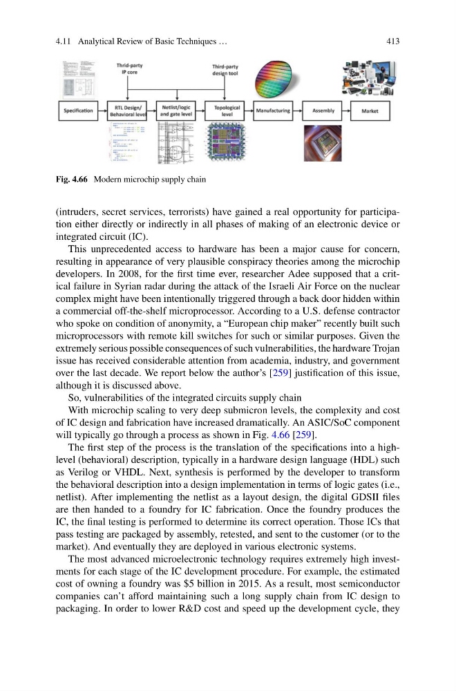
Fig. 4.66 Modern microchip supply chain
(intruders, secret services, terrorists) have gained a real opportunity for participation either directly or indirectly in all phases of making of an electronic device or
integrated circuit (IC).
This unprecedented access to hardware has been a major cause for concern,
resulting in appearance of very plausible conspiracy theories among the microchip
developers. In 2008, for the first time ever, researcher Adee supposed that a critical failure in Syrian radar during the attack of the Israeli Air Force on the nuclear
complex might have been intentionally triggered through a back door hidden within
a commercial off-the-shelf microprocessor. According to a U.S. defense contractor
who spoke on condition of anonymity, a “European chip maker” recently built such
microprocessors with remote kill switches for such or similar purposes. Given the
extremely serious possible consequences of such vulnerabilities, the hardware Trojan
issue has received considerable attention from academia, industry, and government
over the last decade. We report below the author’s [259] justification of this issue,
although it is discussed above.
So, vulnerabilities of the integrated circuits supply chain
With microchip scaling to very deep submicron levels, the complexity and cost
of IC design and fabrication have increased dramatically. An ASIC/SoC component
will typically go through a process as shown in Fig. 4.66 [259].
The first step of the process is the translation of the specifications into a highlevel (behavioral) description, typically in a hardware design language (HDL) such
as Verilog or VHDL. Next, synthesis is performed by the developer to transform
the behavioral description into a design implementation in terms of logic gates (i.e.,
netlist). After implementing the netlist as a layout design, the digital GDSII files
are then handed to a foundry for IC fabrication. Once the foundry produces the
IC, the final testing is performed to determine its correct operation. Those ICs that
pass testing are packaged by assembly, retested, and sent to the customer (or to the
market). And eventually they are deployed in various electronic systems.
The most advanced microelectronic technology requires extremely high investments for each stage of the IC development procedure. For example, the estimated
cost of owning a foundry was $5 billion in 2015. As a result, most semiconductor
companies can’t afford maintaining such a long supply chain from IC design to
packaging. In order to lower R&D cost and speed up the development cycle, they
413
Fig. 4.66 Modern microchip supply chain
(intruders, secret services, terrorists) have gained a real opportunity for participation either directly or indirectly in all phases of making of an electronic device or
integrated circuit (IC).
This unprecedented access to hardware has been a major cause for concern,
resulting in appearance of very plausible conspiracy theories among the microchip
developers. In 2008, for the first time ever, researcher Adee supposed that a critical failure in Syrian radar during the attack of the Israeli Air Force on the nuclear
complex might have been intentionally triggered through a back door hidden within
a commercial off-the-shelf microprocessor. According to a U.S. defense contractor
who spoke on condition of anonymity, a “European chip maker” recently built such
microprocessors with remote kill switches for such or similar purposes. Given the
extremely serious possible consequences of such vulnerabilities, the hardware Trojan
issue has received considerable attention from academia, industry, and government
over the last decade. We report below the author’s [259] justification of this issue,
although it is discussed above.
So, vulnerabilities of the integrated circuits supply chain
With microchip scaling to very deep submicron levels, the complexity and cost
of IC design and fabrication have increased dramatically. An ASIC/SoC component
will typically go through a process as shown in Fig. 4.66 [259].
The first step of the process is the translation of the specifications into a highlevel (behavioral) description, typically in a hardware design language (HDL) such
as Verilog or VHDL. Next, synthesis is performed by the developer to transform
the behavioral description into a design implementation in terms of logic gates (i.e.,
netlist). After implementing the netlist as a layout design, the digital GDSII files
are then handed to a foundry for IC fabrication. Once the foundry produces the
IC, the final testing is performed to determine its correct operation. Those ICs that
pass testing are packaged by assembly, retested, and sent to the customer (or to the
market). And eventually they are deployed in various electronic systems.
The most advanced microelectronic technology requires extremely high investments for each stage of the IC development procedure. For example, the estimated
cost of owning a foundry was $5 billion in 2015. As a result, most semiconductor
companies can’t afford maintaining such a long supply chain from IC design to
packaging. In order to lower R&D cost and speed up the development cycle, they