

388
4 Hardware Trojans in Microcircuits
driver amplifiers (DA). The UWB transmitter is in active mode and transmits a highfrequency signal when a bit of transmitted information is 1; otherwise, it is in standby
mode. The fully CMOS design of this UWB transmitter makes it compatible with the
digital part and helps to further reduce the overall power consumption and ultimately
the cost of the chip.
The chip was designed according to the TSMC CL013G 0.13 μm CMOS
process (http://www.mosis.com/products/fab/vendors/tsmc/tsmc013-cl). The digital
part operates at 75 MHz, and the UWB transmitter has a data transmission speed that
exceeds 50 Mb/s. As is commonly practiced in SoC with mixed signals, test plans
include separate procedures for the digital and analog parts. For the digital part, these
tests cover faults both in delays and constants, using a full scan chain of specially
enhanced scanning triggers. For the analog part, in addition to tests according to the
standard specification, the spectrum of the sequence of output pulses from a chain
of driver amplifiers at a data transmission speed of 50 MB/s was measured. Tests
for operation at the system level additionally included a large number of patterns
that are randomly generated, encrypted, and forwarded by the UWB transmitter. The
receiver decodes ciphertext and compares it with the expected plaintext to recognize
any inconsistencies caused by faults created during manufacturing.
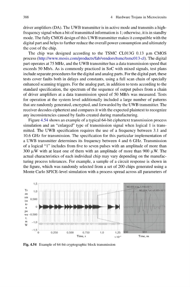
Figure 4.54 shows an example of a typical 64-bit ciphertext transmission process
simulation and an “enlarged” type of transmission signal when logical 1 is transmitted. The UWB specification requires the use of a frequency between 3.1 and
10.6 GHz for transmission. The specification for this particular implementation of
a UWB transmitter determines its frequency between 4 and 6 GHz. Transmission
of a logical “1” includes from five to seven pulses with an amplitude of more than
300 μW with at least one of them with an amplitude of more than 900 μW. The
actual characteristics of each individual chip may vary depending on the manufacturing process tolerances. For example, a sample of a circuit response is shown in
the figure, which was randomly selected from a set of 200 chips generated using a
Monte Carlo SPICE-level simulation with a process spread across all parameters of
Tr
an
sm
iss
io
n
po
we
r,
m
W
Time, s
Time, ns
Fig. 4.54 Example of 64-bit cryptographic block transmission
4 Hardware Trojans in Microcircuits
driver amplifiers (DA). The UWB transmitter is in active mode and transmits a highfrequency signal when a bit of transmitted information is 1; otherwise, it is in standby
mode. The fully CMOS design of this UWB transmitter makes it compatible with the
digital part and helps to further reduce the overall power consumption and ultimately
the cost of the chip.
The chip was designed according to the TSMC CL013G 0.13 μm CMOS
process (http://www.mosis.com/products/fab/vendors/tsmc/tsmc013-cl). The digital
part operates at 75 MHz, and the UWB transmitter has a data transmission speed that
exceeds 50 Mb/s. As is commonly practiced in SoC with mixed signals, test plans
include separate procedures for the digital and analog parts. For the digital part, these
tests cover faults both in delays and constants, using a full scan chain of specially
enhanced scanning triggers. For the analog part, in addition to tests according to the
standard specification, the spectrum of the sequence of output pulses from a chain
of driver amplifiers at a data transmission speed of 50 MB/s was measured. Tests
for operation at the system level additionally included a large number of patterns
that are randomly generated, encrypted, and forwarded by the UWB transmitter. The
receiver decodes ciphertext and compares it with the expected plaintext to recognize
any inconsistencies caused by faults created during manufacturing.
Figure 4.54 shows an example of a typical 64-bit ciphertext transmission process
simulation and an “enlarged” type of transmission signal when logical 1 is transmitted. The UWB specification requires the use of a frequency between 3.1 and
10.6 GHz for transmission. The specification for this particular implementation of
a UWB transmitter determines its frequency between 4 and 6 GHz. Transmission
of a logical “1” includes from five to seven pulses with an amplitude of more than
300 μW with at least one of them with an amplitude of more than 900 μW. The
actual characteristics of each individual chip may vary depending on the manufacturing process tolerances. For example, a sample of a circuit response is shown in
the figure, which was randomly selected from a set of 200 chips generated using a
Monte Carlo SPICE-level simulation with a process spread across all parameters of
Tr
an
sm
iss
io
n
po
we
r,
m
W
Time, s
Time, ns
Fig. 4.54 Example of 64-bit cryptographic block transmission