

4.9 Hardware Trojans in Wireless Cryptographic ICs
387
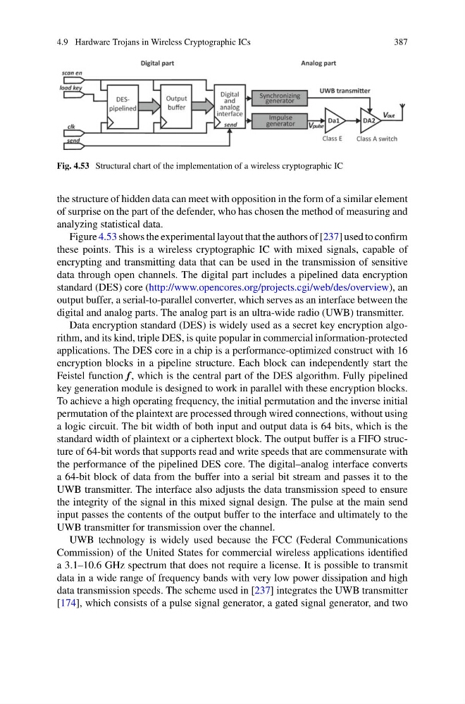
Fig. 4.53 Structural chart of the implementation of a wireless cryptographic IC
the structure of hidden data can meet with opposition in the form of a similar element
of surprise on the part of the defender, who has chosen the method of measuring and
analyzing statistical data.
Figure 4.53 shows the experimental layout that the authors of [237] used to confirm
these points. This is a wireless cryptographic IC with mixed signals, capable of
encrypting and transmitting data that can be used in the transmission of sensitive
data through open channels. The digital part includes a pipelined data encryption
standard (DES) core (http://www.opencores.org/projects.cgi/web/des/overview), an
output buffer, a serial-to-parallel converter, which serves as an interface between the
digital and analog parts. The analog part is an ultra-wide radio (UWB) transmitter.
Data encryption standard (DES) is widely used as a secret key encryption algorithm, and its kind, triple DES, is quite popular in commercial information-protected
applications. The DES core in a chip is a performance-optimized construct with 16
encryption blocks in a pipeline structure. Each block can independently start the
Feistel function f , which is the central part of the DES algorithm. Fully pipelined
key generation module is designed to work in parallel with these encryption blocks.
To achieve a high operating frequency, the initial permutation and the inverse initial
permutation of the plaintext are processed through wired connections, without using
a logic circuit. The bit width of both input and output data is 64 bits, which is the
standard width of plaintext or a ciphertext block. The output buffer is a FIFO structure of 64-bit words that supports read and write speeds that are commensurate with
the performance of the pipelined DES core. The digital–analog interface converts
a 64-bit block of data from the buffer into a serial bit stream and passes it to the
UWB transmitter. The interface also adjusts the data transmission speed to ensure
the integrity of the signal in this mixed signal design. The pulse at the main send
input passes the contents of the output buffer to the interface and ultimately to the
UWB transmitter for transmission over the channel.
UWB technology is widely used because the FCC (Federal Communications
Commission) of the United States for commercial wireless applications identified
a 3.1–10.6 GHz spectrum that does not require a license. It is possible to transmit
data in a wide range of frequency bands with very low power dissipation and high
data transmission speeds. The scheme used in [237] integrates the UWB transmitter
[174], which consists of a pulse signal generator, a gated signal generator, and two
387
Fig. 4.53 Structural chart of the implementation of a wireless cryptographic IC
the structure of hidden data can meet with opposition in the form of a similar element
of surprise on the part of the defender, who has chosen the method of measuring and
analyzing statistical data.
Figure 4.53 shows the experimental layout that the authors of [237] used to confirm
these points. This is a wireless cryptographic IC with mixed signals, capable of
encrypting and transmitting data that can be used in the transmission of sensitive
data through open channels. The digital part includes a pipelined data encryption
standard (DES) core (http://www.opencores.org/projects.cgi/web/des/overview), an
output buffer, a serial-to-parallel converter, which serves as an interface between the
digital and analog parts. The analog part is an ultra-wide radio (UWB) transmitter.
Data encryption standard (DES) is widely used as a secret key encryption algorithm, and its kind, triple DES, is quite popular in commercial information-protected
applications. The DES core in a chip is a performance-optimized construct with 16
encryption blocks in a pipeline structure. Each block can independently start the
Feistel function f , which is the central part of the DES algorithm. Fully pipelined
key generation module is designed to work in parallel with these encryption blocks.
To achieve a high operating frequency, the initial permutation and the inverse initial
permutation of the plaintext are processed through wired connections, without using
a logic circuit. The bit width of both input and output data is 64 bits, which is the
standard width of plaintext or a ciphertext block. The output buffer is a FIFO structure of 64-bit words that supports read and write speeds that are commensurate with
the performance of the pipelined DES core. The digital–analog interface converts
a 64-bit block of data from the buffer into a serial bit stream and passes it to the
UWB transmitter. The interface also adjusts the data transmission speed to ensure
the integrity of the signal in this mixed signal design. The pulse at the main send
input passes the contents of the output buffer to the interface and ultimately to the
UWB transmitter for transmission over the channel.
UWB technology is widely used because the FCC (Federal Communications
Commission) of the United States for commercial wireless applications identified
a 3.1–10.6 GHz spectrum that does not require a license. It is possible to transmit
data in a wide range of frequency bands with very low power dissipation and high
data transmission speeds. The scheme used in [237] integrates the UWB transmitter
[174], which consists of a pulse signal generator, a gated signal generator, and two