

446
M. N. Bojnordi and P. Behnam
w
out
b
b
w
w = { 1 Vdd
0 Gnd
b = { 1 Low Resistance
0 High Resistance
w b out
0 0
1
0 1
0
1 0
0
1 1
1
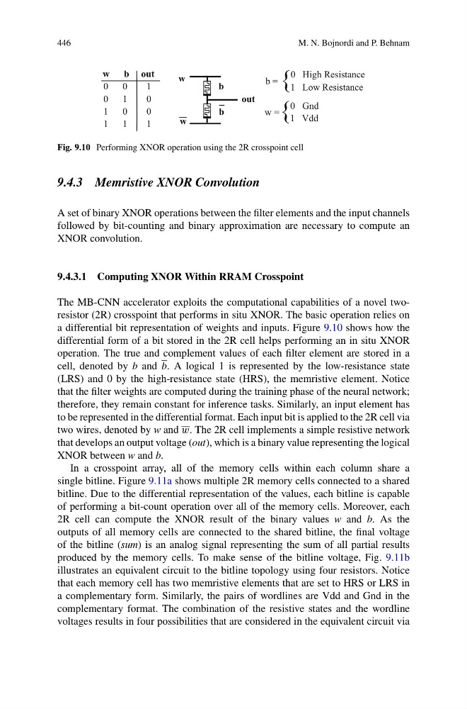
Fig. 9.10 Performing XNOR operation using the 2R crosspoint cell
9.4.3 Memristive XNOR Convolution
A set of binary XNOR operations between the filter elements and the input channels
followed by bit-counting and binary approximation are necessary to compute an
XNOR convolution.
9.4.3.1 Computing XNOR Within RRAM Crosspoint
The MB-CNN accelerator exploits the computational capabilities of a novel tworesistor (2R) crosspoint that performs in situ XNOR. The basic operation relies on
a differential bit representation of weights and inputs. Figure 9.10 shows how the
differential form of a bit stored in the 2R cell helps performing an in situ XNOR
operation. The true and complement values of each filter element are stored in a
cell, denoted by b and b. A logical 1 is represented by the low-resistance state
(LRS) and 0 by the high-resistance state (HRS), the memristive element. Notice
that the filter weights are computed during the training phase of the neural network;
therefore, they remain constant for inference tasks. Similarly, an input element has
to be represented in the differential format. Each input bit is applied to the 2R cell via
two wires, denoted by w and w. The 2R cell implements a simple resistive network
that develops an output voltage (out), which is a binary value representing the logical
XNOR between w and b.
In a crosspoint array, all of the memory cells within each column share a
single bitline. Figure 9.11a shows multiple 2R memory cells connected to a shared
bitline. Due to the differential representation of the values, each bitline is capable
of performing a bit-count operation over all of the memory cells. Moreover, each
2R cell can compute the XNOR result of the binary values w and b. As the
outputs of all memory cells are connected to the shared bitline, the final voltage
of the bitline (sum) is an analog signal representing the sum of all partial results
produced by the memory cells. To make sense of the bitline voltage, Fig. 9.11b
illustrates an equivalent circuit to the bitline topology using four resistors. Notice
that each memory cell has two memristive elements that are set to HRS or LRS in
a complementary form. Similarly, the pairs of wordlines are Vdd and Gnd in the
complementary format. The combination of the resistive states and the wordline
voltages results in four possibilities that are considered in the equivalent circuit via
M. N. Bojnordi and P. Behnam
w
out
b
b
w
w = { 1 Vdd
0 Gnd
b = { 1 Low Resistance
0 High Resistance
w b out
0 0
1
0 1
0
1 0
0
1 1
1
Fig. 9.10 Performing XNOR operation using the 2R crosspoint cell
9.4.3 Memristive XNOR Convolution
A set of binary XNOR operations between the filter elements and the input channels
followed by bit-counting and binary approximation are necessary to compute an
XNOR convolution.
9.4.3.1 Computing XNOR Within RRAM Crosspoint
The MB-CNN accelerator exploits the computational capabilities of a novel tworesistor (2R) crosspoint that performs in situ XNOR. The basic operation relies on
a differential bit representation of weights and inputs. Figure 9.10 shows how the
differential form of a bit stored in the 2R cell helps performing an in situ XNOR
operation. The true and complement values of each filter element are stored in a
cell, denoted by b and b. A logical 1 is represented by the low-resistance state
(LRS) and 0 by the high-resistance state (HRS), the memristive element. Notice
that the filter weights are computed during the training phase of the neural network;
therefore, they remain constant for inference tasks. Similarly, an input element has
to be represented in the differential format. Each input bit is applied to the 2R cell via
two wires, denoted by w and w. The 2R cell implements a simple resistive network
that develops an output voltage (out), which is a binary value representing the logical
XNOR between w and b.
In a crosspoint array, all of the memory cells within each column share a
single bitline. Figure 9.11a shows multiple 2R memory cells connected to a shared
bitline. Due to the differential representation of the values, each bitline is capable
of performing a bit-count operation over all of the memory cells. Moreover, each
2R cell can compute the XNOR result of the binary values w and b. As the
outputs of all memory cells are connected to the shared bitline, the final voltage
of the bitline (sum) is an analog signal representing the sum of all partial results
produced by the memory cells. To make sense of the bitline voltage, Fig. 9.11b
illustrates an equivalent circuit to the bitline topology using four resistors. Notice
that each memory cell has two memristive elements that are set to HRS or LRS in
a complementary form. Similarly, the pairs of wordlines are Vdd and Gnd in the
complementary format. The combination of the resistive states and the wordline
voltages results in four possibilities that are considered in the equivalent circuit via