

92
F. Firouzi et al.
2.5.9 Programming and Debugging Techniques
There are a few main techniques available to program a microcontroller, namely,
JTAG/SWD and Bootloader. Outlined below are the benefits and drawbacks of each
method [17].
2.5.9.1 JTAG/SWD
Joint Test Action Group (JTAG) is an industry standard initially designed for
electrical testing of integrated circuits after manufacturing by means of boundary
scanning mechanisms. Since then, JTAG has evolved into a common interface
utilized to control the entire microcontroller and is currently used to program, test,
and debug almost all embedded devices. A complete JTAG interface needs the five
pins indicated below:
• Test Mode Select (TMS) – This signal is used to determine the next state of the
system.
• Test Clock (TCK) – Clock of the system during test/debug mode.
• Test Data Input (TDI) – The input data that is shifted into the device.
• Test Data Output (TDO) – The output data that is shifted out of the device.
• Test Reset (TRST) – Rest pin to reset the JTAG controller system.
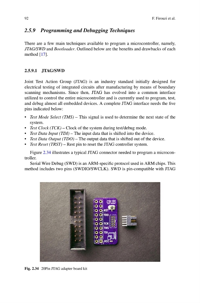
Figure 2.34 illustrates a typical JTAG connector needed to program a microcontroller.
Serial Wire Debug (SWD) is an ARM-specific protocol used in ARM chips. This
method includes two pins (SWDIO/SWCLK). SWD is pin-compatible with JTAG
Fig. 2.34 20Pin JTAG adapter board kit
F. Firouzi et al.
2.5.9 Programming and Debugging Techniques
There are a few main techniques available to program a microcontroller, namely,
JTAG/SWD and Bootloader. Outlined below are the benefits and drawbacks of each
method [17].
2.5.9.1 JTAG/SWD
Joint Test Action Group (JTAG) is an industry standard initially designed for
electrical testing of integrated circuits after manufacturing by means of boundary
scanning mechanisms. Since then, JTAG has evolved into a common interface
utilized to control the entire microcontroller and is currently used to program, test,
and debug almost all embedded devices. A complete JTAG interface needs the five
pins indicated below:
• Test Mode Select (TMS) – This signal is used to determine the next state of the
system.
• Test Clock (TCK) – Clock of the system during test/debug mode.
• Test Data Input (TDI) – The input data that is shifted into the device.
• Test Data Output (TDO) – The output data that is shifted out of the device.
• Test Reset (TRST) – Rest pin to reset the JTAG controller system.
Figure 2.34 illustrates a typical JTAG connector needed to program a microcontroller.
Serial Wire Debug (SWD) is an ARM-specific protocol used in ARM chips. This
method includes two pins (SWDIO/SWCLK). SWD is pin-compatible with JTAG
Fig. 2.34 20Pin JTAG adapter board kit