

80
M. Zhong and P. Fan
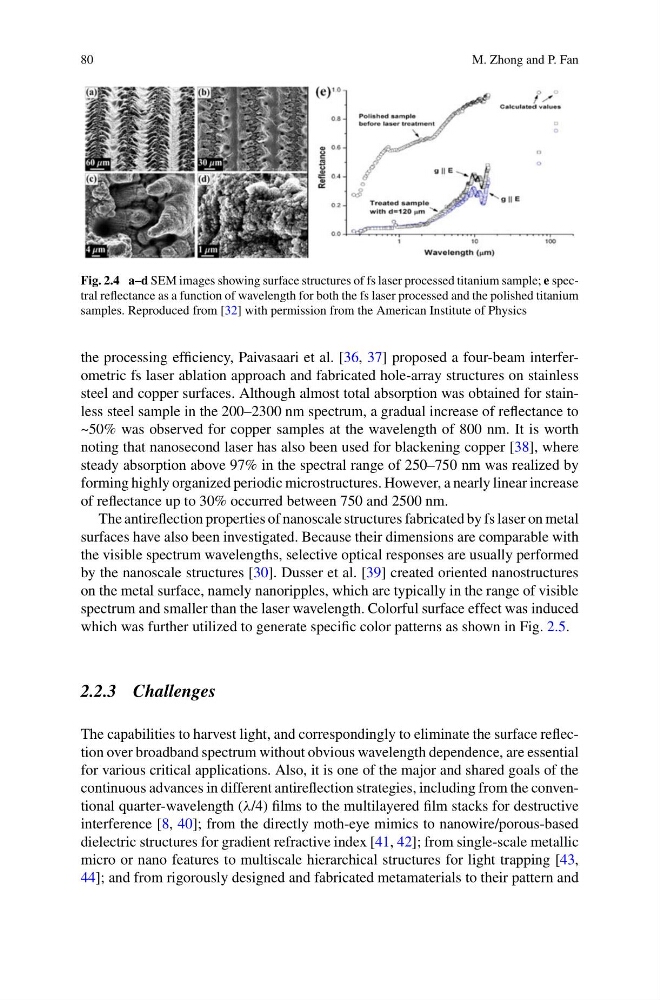
Fig. 2.4 a–d SEM images showing surface structures of fs laser processed titanium sample; e spectral reflectance as a function of wavelength for both the fs laser processed and the polished titanium
samples. Reproduced from [32] with permission from the American Institute of Physics
the processing efficiency, Paivasaari et al. [36, 37] proposed a four-beam interferometric fs laser ablation approach and fabricated hole-array structures on stainless
steel and copper surfaces. Although almost total absorption was obtained for stainless steel sample in the 200–2300 nm spectrum, a gradual increase of reflectance to
~50% was observed for copper samples at the wavelength of 800 nm. It is worth
noting that nanosecond laser has also been used for blackening copper [38], where
steady absorption above 97% in the spectral range of 250–750 nm was realized by
forming highly organized periodic microstructures. However, a nearly linear increase
of reflectance up to 30% occurred between 750 and 2500 nm.
The antireflection properties of nanoscale structures fabricated by fs laser on metal
surfaces have also been investigated. Because their dimensions are comparable with
the visible spectrum wavelengths, selective optical responses are usually performed
by the nanoscale structures [30]. Dusser et al. [39] created oriented nanostructures
on the metal surface, namely nanoripples, which are typically in the range of visible
spectrum and smaller than the laser wavelength. Colorful surface effect was induced
which was further utilized to generate specific color patterns as shown in Fig. 2.5.
2.2.3 Challenges
The capabilities to harvest light, and correspondingly to eliminate the surface reflection over broadband spectrum without obvious wavelength dependence, are essential
for various critical applications. Also, it is one of the major and shared goals of the
continuous advances in different antireflection strategies, including from the conventional quarter-wavelength (λ/4) films to the multilayered film stacks for destructive
interference [8, 40]; from the directly moth-eye mimics to nanowire/porous-based
dielectric structures for gradient refractive index [41, 42]; from single-scale metallic
micro or nano features to multiscale hierarchical structures for light trapping [43,
44]; and from rigorously designed and fabricated metamaterials to their pattern and
M. Zhong and P. Fan
Fig. 2.4 a–d SEM images showing surface structures of fs laser processed titanium sample; e spectral reflectance as a function of wavelength for both the fs laser processed and the polished titanium
samples. Reproduced from [32] with permission from the American Institute of Physics
the processing efficiency, Paivasaari et al. [36, 37] proposed a four-beam interferometric fs laser ablation approach and fabricated hole-array structures on stainless
steel and copper surfaces. Although almost total absorption was obtained for stainless steel sample in the 200–2300 nm spectrum, a gradual increase of reflectance to
~50% was observed for copper samples at the wavelength of 800 nm. It is worth
noting that nanosecond laser has also been used for blackening copper [38], where
steady absorption above 97% in the spectral range of 250–750 nm was realized by
forming highly organized periodic microstructures. However, a nearly linear increase
of reflectance up to 30% occurred between 750 and 2500 nm.
The antireflection properties of nanoscale structures fabricated by fs laser on metal
surfaces have also been investigated. Because their dimensions are comparable with
the visible spectrum wavelengths, selective optical responses are usually performed
by the nanoscale structures [30]. Dusser et al. [39] created oriented nanostructures
on the metal surface, namely nanoripples, which are typically in the range of visible
spectrum and smaller than the laser wavelength. Colorful surface effect was induced
which was further utilized to generate specific color patterns as shown in Fig. 2.5.
2.2.3 Challenges
The capabilities to harvest light, and correspondingly to eliminate the surface reflection over broadband spectrum without obvious wavelength dependence, are essential
for various critical applications. Also, it is one of the major and shared goals of the
continuous advances in different antireflection strategies, including from the conventional quarter-wavelength (λ/4) films to the multilayered film stacks for destructive
interference [8, 40]; from the directly moth-eye mimics to nanowire/porous-based
dielectric structures for gradient refractive index [41, 42]; from single-scale metallic
micro or nano features to multiscale hierarchical structures for light trapping [43,
44]; and from rigorously designed and fabricated metamaterials to their pattern and