

1 Introduction to Laser Micro-to-Nano Manufacturing
41
lens), and translation motorized stage (multi-axis platform). Using high numerical -
aperture objective lens and piezo stage stages, laser direct wiring have the fabrication
resolution down to the sub-micrometer dimension.
Laser Interference Lithography Although laser direct writing has advantages as
the aforementioned, laser interference lithography is suitable for the fabrication of
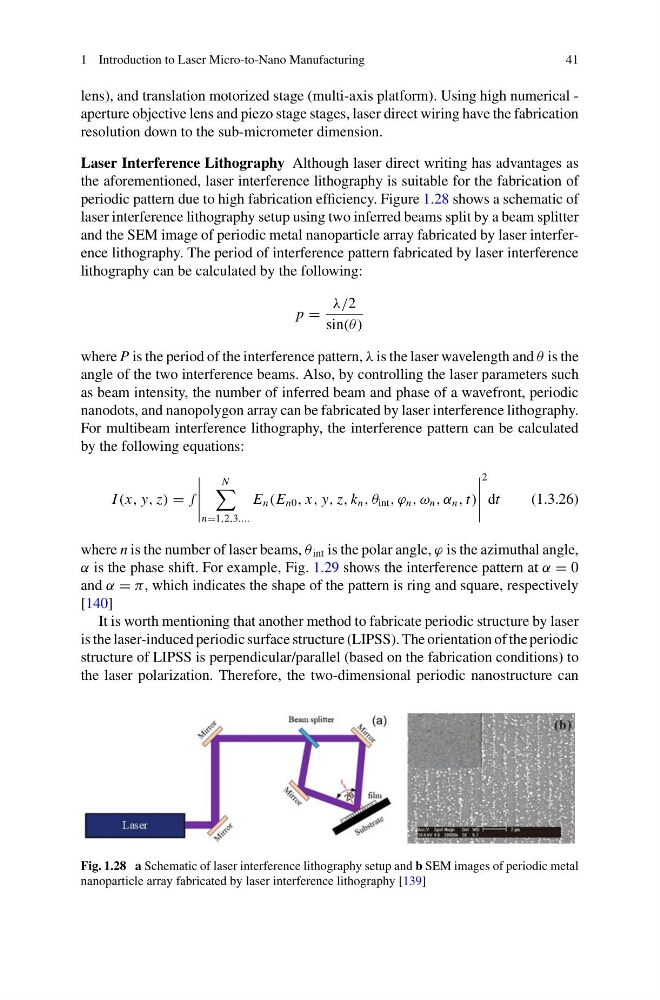
periodic pattern due to high fabrication efficiency. Figure 1.28 shows a schematic of
laser interference lithography setup using two inferred beams split by a beam splitter
and the SEM image of periodic metal nanoparticle array fabricated by laser interference lithography. The period of interference pattern fabricated by laser interference
lithography can be calculated by the following:
p =
λ/2
sin(θ )
where P is the period of the interference pattern, λ is the laser wavelength and θ is the
angle of the two interference beams. Also, by controlling the laser parameters such
as beam intensity, the number of inferred beam and phase of a wavefront, periodic
nanodots, and nanopolygon array can be fabricated by laser interference lithography.
For multibeam interference lithography, the interference pattern can be calculated
by the following equations:
I (x, y, z) = ∫
N
n=1,2,3....
E n (E n0 , x, y, z, k n , θ int , ϕ n , ω n , α n , t)
2
dt
(1.3.26)
where n is the number of laser beams, θ int is the polar angle, ϕ is the azimuthal angle,
α is the phase shift. For example, Fig. 1.29 shows the interference pattern at α = 0
and α = π, which indicates the shape of the pattern is ring and square, respectively
[140]
It is worth mentioning that another method to fabricate periodic structure by laser
is the laser-induced periodic surface structure (LIPSS). The orientation of the periodic
structure of LIPSS is perpendicular/parallel (based on the fabrication conditions) to
the laser polarization. Therefore, the two-dimensional periodic nanostructure can
Fig. 1.28 a Schematic of laser interference lithography setup and b SEM images of periodic metal
nanoparticle array fabricated by laser interference lithography [139]
41
lens), and translation motorized stage (multi-axis platform). Using high numerical -
aperture objective lens and piezo stage stages, laser direct wiring have the fabrication
resolution down to the sub-micrometer dimension.
Laser Interference Lithography Although laser direct writing has advantages as
the aforementioned, laser interference lithography is suitable for the fabrication of
periodic pattern due to high fabrication efficiency. Figure 1.28 shows a schematic of
laser interference lithography setup using two inferred beams split by a beam splitter
and the SEM image of periodic metal nanoparticle array fabricated by laser interference lithography. The period of interference pattern fabricated by laser interference
lithography can be calculated by the following:
p =
λ/2
sin(θ )
where P is the period of the interference pattern, λ is the laser wavelength and θ is the
angle of the two interference beams. Also, by controlling the laser parameters such
as beam intensity, the number of inferred beam and phase of a wavefront, periodic
nanodots, and nanopolygon array can be fabricated by laser interference lithography.
For multibeam interference lithography, the interference pattern can be calculated
by the following equations:
I (x, y, z) = ∫
N
n=1,2,3....
E n (E n0 , x, y, z, k n , θ int , ϕ n , ω n , α n , t)
2
dt
(1.3.26)
where n is the number of laser beams, θ int is the polar angle, ϕ is the azimuthal angle,
α is the phase shift. For example, Fig. 1.29 shows the interference pattern at α = 0
and α = π, which indicates the shape of the pattern is ring and square, respectively
[140]
It is worth mentioning that another method to fabricate periodic structure by laser
is the laser-induced periodic surface structure (LIPSS). The orientation of the periodic
structure of LIPSS is perpendicular/parallel (based on the fabrication conditions) to
the laser polarization. Therefore, the two-dimensional periodic nanostructure can
Fig. 1.28 a Schematic of laser interference lithography setup and b SEM images of periodic metal
nanoparticle array fabricated by laser interference lithography [139]