

28
A. Hu et al.
underlying diffusion. It is possible to identify these mechanisms by characterizing
the neck variation as a function of time. Nevertheless, there is limited experimental
analyses by these models. The molecular dynamics simulations display remarkable
differences from these models [107, 108]. The further investigation is desired to
verify these models at a nanoscale.
It is extensively to use a pulsed light rather than a continue wave (constant) light
for photonic sintering. With a constant energy output, a pulsed laser indicates a
higher peak, which allows a deep penetration since the penetration is proportional to
the input power. Besides, the pulsed laser allows the photothermal energy dissipation
with a pulse gap for cooling. For sintering of printed circuit with pulsed light, because
of the absorption difference of printed materials and substrates, it is possible to limit
the thermal effect on the oriented layer only by choosing the proper wavelength. The
metallic particles mainly absorb a visible or infrared light while the plastic/paper
absorbs a ultraviolet light. It is thus reasonable to use a long-wavelength light for
photonic sintering to avoid the thermal accumulation onto the plastic/paper substrate.
This feature has advantage because one can print circuits onto a cheap plastic and/or
paper substrates for flexible and/or stretchable devices for wearable/portable electronics [101, 109]. On the other hand, it is worth noting that the plasmonic resonant
frequency is proportional to the anisotropy of nanomaterials. This means that the
resonant wavelength has a blue-shift while the sintering processing [5, 75]. Thus, if
the photonic sintering is completed by integrating different light sources, one should
put a longer light sources before a short light source. Figure 1.22 shows a practical
photonic sintering system by combining three kinds of pulsed light for sintering of
printed Cu circuits [110].
The single sintering will gradually lead to the decrease of resistance. However, due
to the inhomogeneous distribution of grain size as well as the diffusion is influenced
by grain orientations and impurity on the grain boundaries, it is naturally predicted
that there are large variation of local resistivity [111]. Thus, the global resistivity
of printed circuits will dependent on several factors including the scattering from
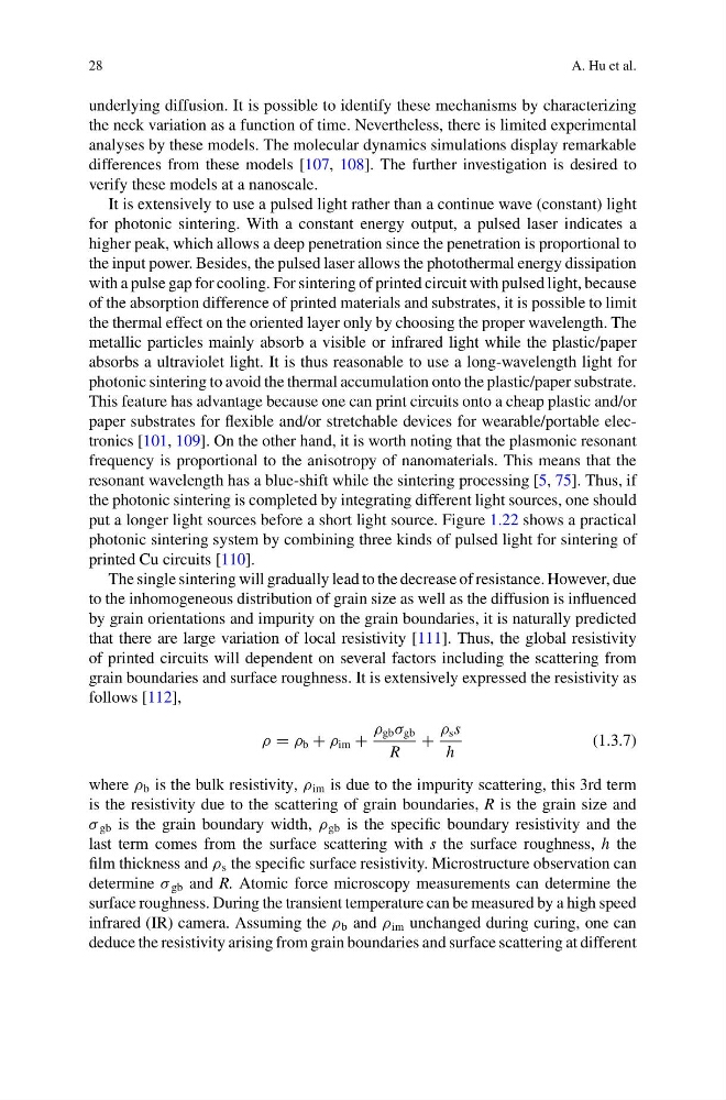
grain boundaries and surface roughness. It is extensively expressed the resistivity as
follows [112],
ρ = ρ b + ρ im +
ρ gb σ gb
R
+
ρ s s
h
(1.3.7)
where ρ b is the bulk resistivity, ρ im is due to the impurity scattering, this 3rd term
is the resistivity due to the scattering of grain boundaries, R is the grain size and
σ gb is the grain boundary width, ρ gb is the specific boundary resistivity and the
last term comes from the surface scattering with s the surface roughness, h the
film thickness and ρ s the specific surface resistivity. Microstructure observation can
determine σ gb and R. Atomic force microscopy measurements can determine the
surface roughness. During the transient temperature can be measured by a high speed
infrared (IR) camera. Assuming the ρ b and ρ im unchanged during curing, one can
deduce the resistivity arising from grain boundaries and surface scattering at different
A. Hu et al.
underlying diffusion. It is possible to identify these mechanisms by characterizing
the neck variation as a function of time. Nevertheless, there is limited experimental
analyses by these models. The molecular dynamics simulations display remarkable
differences from these models [107, 108]. The further investigation is desired to
verify these models at a nanoscale.
It is extensively to use a pulsed light rather than a continue wave (constant) light
for photonic sintering. With a constant energy output, a pulsed laser indicates a
higher peak, which allows a deep penetration since the penetration is proportional to
the input power. Besides, the pulsed laser allows the photothermal energy dissipation
with a pulse gap for cooling. For sintering of printed circuit with pulsed light, because
of the absorption difference of printed materials and substrates, it is possible to limit
the thermal effect on the oriented layer only by choosing the proper wavelength. The
metallic particles mainly absorb a visible or infrared light while the plastic/paper
absorbs a ultraviolet light. It is thus reasonable to use a long-wavelength light for
photonic sintering to avoid the thermal accumulation onto the plastic/paper substrate.
This feature has advantage because one can print circuits onto a cheap plastic and/or
paper substrates for flexible and/or stretchable devices for wearable/portable electronics [101, 109]. On the other hand, it is worth noting that the plasmonic resonant
frequency is proportional to the anisotropy of nanomaterials. This means that the
resonant wavelength has a blue-shift while the sintering processing [5, 75]. Thus, if
the photonic sintering is completed by integrating different light sources, one should
put a longer light sources before a short light source. Figure 1.22 shows a practical
photonic sintering system by combining three kinds of pulsed light for sintering of
printed Cu circuits [110].
The single sintering will gradually lead to the decrease of resistance. However, due
to the inhomogeneous distribution of grain size as well as the diffusion is influenced
by grain orientations and impurity on the grain boundaries, it is naturally predicted
that there are large variation of local resistivity [111]. Thus, the global resistivity
of printed circuits will dependent on several factors including the scattering from
grain boundaries and surface roughness. It is extensively expressed the resistivity as
follows [112],
ρ = ρ b + ρ im +
ρ gb σ gb
R
+
ρ s s
h
(1.3.7)
where ρ b is the bulk resistivity, ρ im is due to the impurity scattering, this 3rd term
is the resistivity due to the scattering of grain boundaries, R is the grain size and
σ gb is the grain boundary width, ρ gb is the specific boundary resistivity and the
last term comes from the surface scattering with s the surface roughness, h the
film thickness and ρ s the specific surface resistivity. Microstructure observation can
determine σ gb and R. Atomic force microscopy measurements can determine the
surface roughness. During the transient temperature can be measured by a high speed
infrared (IR) camera. Assuming the ρ b and ρ im unchanged during curing, one can
deduce the resistivity arising from grain boundaries and surface scattering at different