

9 Laser-Induced Forward Transfer Towards Additive Manufacturing
295
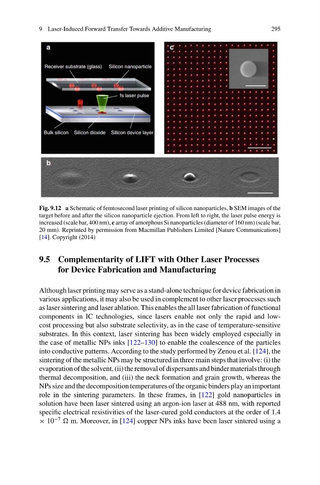
Fig. 9.12 a Schematic of femtosecond laser printing of silicon nanoparticles, b SEM images of the
target before and after the silicon nanoparticle ejection. From left to right, the laser pulse energy is
increased (scale bar, 400 nm), c array of amorphous Si nanoparticles (diameter of 160 nm) (scale bar,
20 mm). Reprinted by permission from Macmillan Publishers Limited [Nature Communications]
[14]. Copyright (2014)
9.5 Complementarity of LIFT with Other Laser Processes
for Device Fabrication and Manufacturing
Although laser printing may serve as a stand-alone technique for device fabrication in
various applications, it may also be used in complement to other laser processes such
as laser sintering and laser ablation. This enables the all laser fabrication of functional
components in IC technologies, since lasers enable not only the rapid and lowcost processing but also substrate selectivity, as in the case of temperature-sensitive
substrates. In this context, laser sintering has been widely employed especially in
the case of metallic NPs inks [122–130] to enable the coalescence of the particles
into conductive patterns. According to the study performed by Zenou et al. [124], the
sintering of the metallic NPs may be structured in three main steps that involve: (i) the
evaporation of the solvent, (ii) the removal of dispersants and binder materials through
thermal decomposition, and (iii) the neck formation and grain growth, whereas the
NPs size and the decomposition temperatures of the organic binders play an important
role in the sintering parameters. In these frames, in [122] gold nanoparticles in
solution have been laser sintered using an argon-ion laser at 488 nm, with reported
specific electrical resistivities of the laser-cured gold conductors at the order of 1.4
× 10
−7
m. Moreover, in [124] copper NPs inks have been laser sintered using a
295
Fig. 9.12 a Schematic of femtosecond laser printing of silicon nanoparticles, b SEM images of the
target before and after the silicon nanoparticle ejection. From left to right, the laser pulse energy is
increased (scale bar, 400 nm), c array of amorphous Si nanoparticles (diameter of 160 nm) (scale bar,
20 mm). Reprinted by permission from Macmillan Publishers Limited [Nature Communications]
[14]. Copyright (2014)
9.5 Complementarity of LIFT with Other Laser Processes
for Device Fabrication and Manufacturing
Although laser printing may serve as a stand-alone technique for device fabrication in
various applications, it may also be used in complement to other laser processes such
as laser sintering and laser ablation. This enables the all laser fabrication of functional
components in IC technologies, since lasers enable not only the rapid and lowcost processing but also substrate selectivity, as in the case of temperature-sensitive
substrates. In this context, laser sintering has been widely employed especially in
the case of metallic NPs inks [122–130] to enable the coalescence of the particles
into conductive patterns. According to the study performed by Zenou et al. [124], the
sintering of the metallic NPs may be structured in three main steps that involve: (i) the
evaporation of the solvent, (ii) the removal of dispersants and binder materials through
thermal decomposition, and (iii) the neck formation and grain growth, whereas the
NPs size and the decomposition temperatures of the organic binders play an important
role in the sintering parameters. In these frames, in [122] gold nanoparticles in
solution have been laser sintered using an argon-ion laser at 488 nm, with reported
specific electrical resistivities of the laser-cured gold conductors at the order of 1.4
× 10
−7
m. Moreover, in [124] copper NPs inks have been laser sintered using a