

9 Laser-Induced Forward Transfer Towards Additive Manufacturing
279
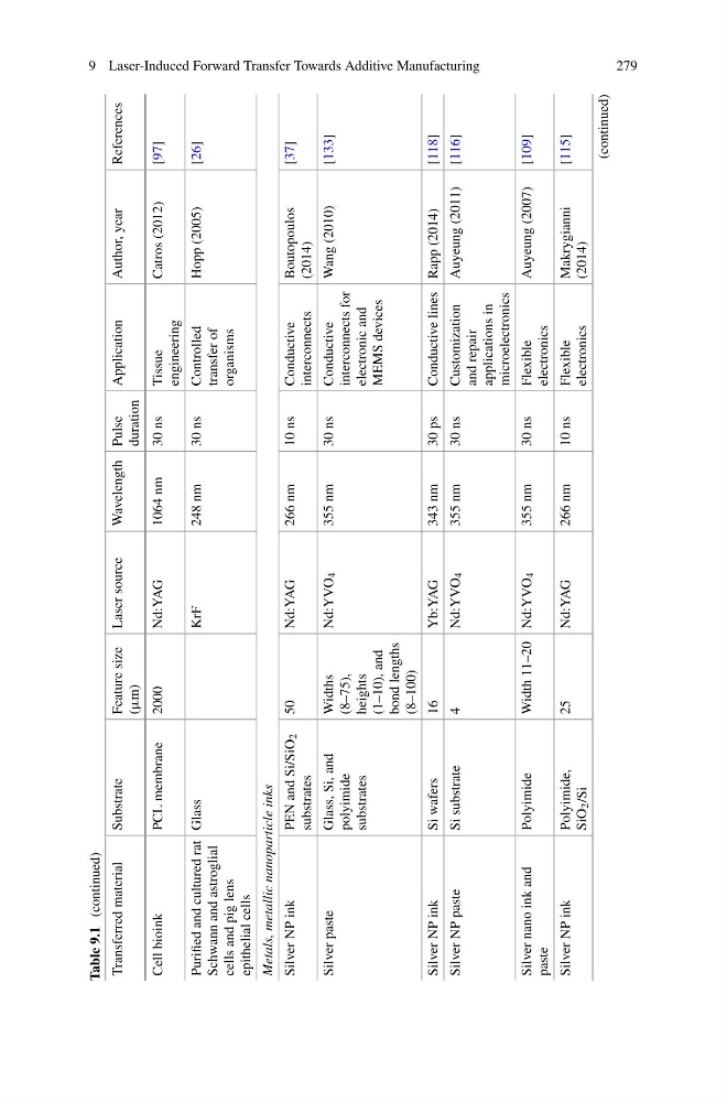
Table 9.1
(continued)
Transferred material
Substrate
Feature size
(µm)
Laser source
Wavelength Pulse
duration
Application
Author, year
References
Cell bioink
PCL membrane
2000
Nd:YAG
1064 nm
30 ns
Tissue
engineering
Catros (2012)
[97]
Purified and cultured rat
Schwann and astroglial
cells and pig lens
epithelial cells
Glass
KrF
248 nm
30 ns
Controlled
transfer of
organisms
Hopp (2005)
[26]
Metals, metallic nanoparticle inks
Silver NP ink
PEN and Si/SiO
2
substrates
50
Nd:YAG
266 nm
10 ns
Conductive
interconnects
Boutopoulos
(2014)
[37]
Silver paste
Glass, Si, and
polyimide
substrates
Widths
(8–75),
heights
(1–10), and
bond lengths
(8–100)
Nd:YVO
4
355 nm
30 ns
Conductive
interconnects for
electronic and
MEMS devices
Wang (2010)
[133]
Silver NP ink
Si wafers
16
Yb:YAG
343 nm
30 ps
Conductive lines Rapp (2014)
[118]
Silver NP paste
Si substrate
4
Nd:YVO
4
355 nm
30 ns
Customization
and repair
applications in
microelectronics
Auyeung (2011)
[116]
Silver nano ink and
paste
Polyimide
Width 11–20 Nd:YVO
4
355 nm
30 ns
Flexible
electronics
Auyeung (2007)
[109]
Silver NP ink
Polyimide,
SiO
2 /Si
25
Nd:YAG
266 nm
10 ns
Flexible
electronics
Makrygianni
(2014)
[115]
(continued)
279
Table 9.1
(continued)
Transferred material
Substrate
Feature size
(µm)
Laser source
Wavelength Pulse
duration
Application
Author, year
References
Cell bioink
PCL membrane
2000
Nd:YAG
1064 nm
30 ns
Tissue
engineering
Catros (2012)
[97]
Purified and cultured rat
Schwann and astroglial
cells and pig lens
epithelial cells
Glass
KrF
248 nm
30 ns
Controlled
transfer of
organisms
Hopp (2005)
[26]
Metals, metallic nanoparticle inks
Silver NP ink
PEN and Si/SiO
2
substrates
50
Nd:YAG
266 nm
10 ns
Conductive
interconnects
Boutopoulos
(2014)
[37]
Silver paste
Glass, Si, and
polyimide
substrates
Widths
(8–75),
heights
(1–10), and
bond lengths
(8–100)
Nd:YVO
4
355 nm
30 ns
Conductive
interconnects for
electronic and
MEMS devices
Wang (2010)
[133]
Silver NP ink
Si wafers
16
Yb:YAG
343 nm
30 ps
Conductive lines Rapp (2014)
[118]
Silver NP paste
Si substrate
4
Nd:YVO
4
355 nm
30 ns
Customization
and repair
applications in
microelectronics
Auyeung (2011)
[116]
Silver nano ink and
paste
Polyimide
Width 11–20 Nd:YVO
4
355 nm
30 ns
Flexible
electronics
Auyeung (2007)
[109]
Silver NP ink
Polyimide,
SiO
2 /Si
25
Nd:YAG
266 nm
10 ns
Flexible
electronics
Makrygianni
(2014)
[115]
(continued)