

236
G. Feng et al.
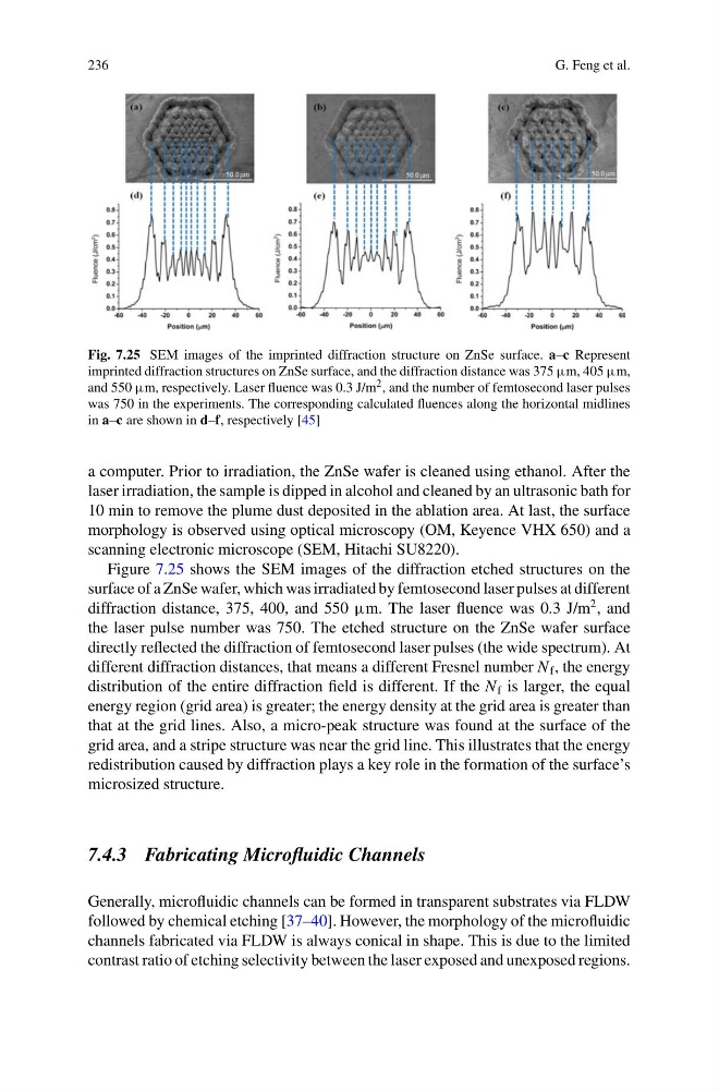
Fig. 7.25 SEM images of the imprinted diffraction structure on ZnSe surface. a–c Represent
imprinted diffraction structures on ZnSe surface, and the diffraction distance was 375 μm, 405 μm,
and 550 μm, respectively. Laser fluence was 0.3 J/m 2 , and the number of femtosecond laser pulses
was 750 in the experiments. The corresponding calculated fluences along the horizontal midlines
in a–c are shown in d–f, respectively [45]
a computer. Prior to irradiation, the ZnSe wafer is cleaned using ethanol. After the
laser irradiation, the sample is dipped in alcohol and cleaned by an ultrasonic bath for
10 min to remove the plume dust deposited in the ablation area. At last, the surface
morphology is observed using optical microscopy (OM, Keyence VHX 650) and a
scanning electronic microscope (SEM, Hitachi SU8220).
Figure 7.25 shows the SEM images of the diffraction etched structures on the
surface of a ZnSe wafer, which was irradiated by femtosecond laser pulses at different
diffraction distance, 375, 400, and 550 μm. The laser fluence was 0.3 J/m
2 , and
the laser pulse number was 750. The etched structure on the ZnSe wafer surface
directly reflected the diffraction of femtosecond laser pulses (the wide spectrum). At
different diffraction distances, that means a different Fresnel number N f , the energy
distribution of the entire diffraction field is different. If the N f is larger, the equal
energy region (grid area) is greater; the energy density at the grid area is greater than
that at the grid lines. Also, a micro-peak structure was found at the surface of the
grid area, and a stripe structure was near the grid line. This illustrates that the energy
redistribution caused by diffraction plays a key role in the formation of the surface’s
microsized structure.
7.4.3 Fabricating Microfluidic Channels
Generally, microfluidic channels can be formed in transparent substrates via FLDW
followed by chemical etching [37–40]. However, the morphology of the microfluidic
channels fabricated via FLDW is always conical in shape. This is due to the limited
contrast ratio of etching selectivity between the laser exposed and unexposed regions.
G. Feng et al.
Fig. 7.25 SEM images of the imprinted diffraction structure on ZnSe surface. a–c Represent
imprinted diffraction structures on ZnSe surface, and the diffraction distance was 375 μm, 405 μm,
and 550 μm, respectively. Laser fluence was 0.3 J/m 2 , and the number of femtosecond laser pulses
was 750 in the experiments. The corresponding calculated fluences along the horizontal midlines
in a–c are shown in d–f, respectively [45]
a computer. Prior to irradiation, the ZnSe wafer is cleaned using ethanol. After the
laser irradiation, the sample is dipped in alcohol and cleaned by an ultrasonic bath for
10 min to remove the plume dust deposited in the ablation area. At last, the surface
morphology is observed using optical microscopy (OM, Keyence VHX 650) and a
scanning electronic microscope (SEM, Hitachi SU8220).
Figure 7.25 shows the SEM images of the diffraction etched structures on the
surface of a ZnSe wafer, which was irradiated by femtosecond laser pulses at different
diffraction distance, 375, 400, and 550 μm. The laser fluence was 0.3 J/m
2 , and
the laser pulse number was 750. The etched structure on the ZnSe wafer surface
directly reflected the diffraction of femtosecond laser pulses (the wide spectrum). At
different diffraction distances, that means a different Fresnel number N f , the energy
distribution of the entire diffraction field is different. If the N f is larger, the equal
energy region (grid area) is greater; the energy density at the grid area is greater than
that at the grid lines. Also, a micro-peak structure was found at the surface of the
grid area, and a stripe structure was near the grid line. This illustrates that the energy
redistribution caused by diffraction plays a key role in the formation of the surface’s
microsized structure.
7.4.3 Fabricating Microfluidic Channels
Generally, microfluidic channels can be formed in transparent substrates via FLDW
followed by chemical etching [37–40]. However, the morphology of the microfluidic
channels fabricated via FLDW is always conical in shape. This is due to the limited
contrast ratio of etching selectivity between the laser exposed and unexposed regions.