

5.2 Polarization Effects in InGaN/GaN Multiple Quantum Wells Materials
81
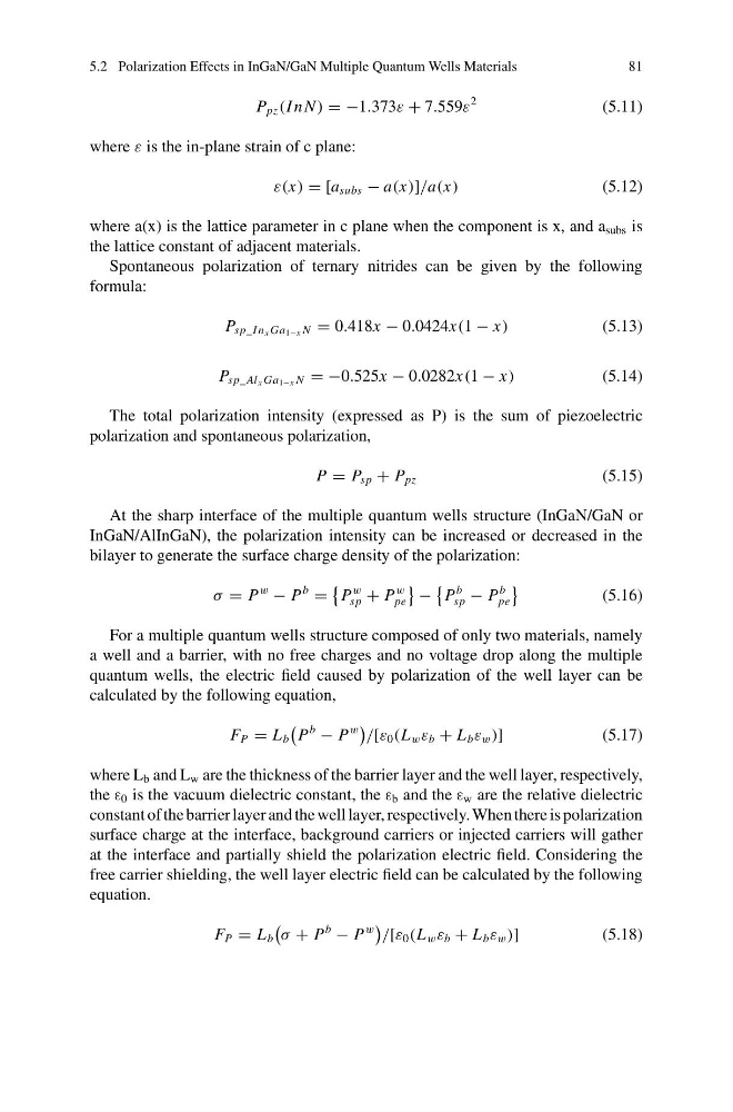
P pz (I nN ) = −1.373ε + 7.559ε
2
(5.11)
where ε is the in-plane strain of c plane:
ε(x) = [a subs − a(x)]/a(x)
(5.12)
where a(x) is the lattice parameter in c plane when the component is x, and a subs is
the lattice constant of adjacent materials.
Spontaneous polarization of ternary nitrides can be given by the following
formula:
P sp_I n x Ga 1−x N = 0.418x − 0.0424x(1 − x)
(5.13)
P sp_ Al x Ga 1−x N = −0.525x − 0.0282x(1 − x)
(5.14)
The total polarization intensity (expressed as P) is the sum of piezoelectric
polarization and spontaneous polarization,
P = P sp + P pz
(5.15)
At the sharp interface of the multiple quantum wells structure (InGaN/GaN or
InGaN/AlInGaN), the polarization intensity can be increased or decreased in the
bilayer to generate the surface charge density of the polarization:
σ = P
w
− P
b
=
P
w
sp + P
w
pe
−
P
b
sp − P
b
pe
(5.16)
For a multiple quantum wells structure composed of only two materials, namely
a well and a barrier, with no free charges and no voltage drop along the multiple
quantum wells, the electric field caused by polarization of the well layer can be
calculated by the following equation,
F P = L b
P
b
− P
w
/[ε 0 (L w ε b + L b ε w )]
(5.17)
where L b and L w are the thickness of the barrier layer and the well layer, respectively,
the ε 0 is the vacuum dielectric constant, the ε b and the ε w are the relative dielectric
constant of the barrier layer and the well layer, respectively. When there is polarization
surface charge at the interface, background carriers or injected carriers will gather
at the interface and partially shield the polarization electric field. Considering the
free carrier shielding, the well layer electric field can be calculated by the following
equation.
F P = L b
σ + P
b
− P
w
/[ε 0 (L w ε b + L b ε w )]
(5.18)
81
P pz (I nN ) = −1.373ε + 7.559ε
2
(5.11)
where ε is the in-plane strain of c plane:
ε(x) = [a subs − a(x)]/a(x)
(5.12)
where a(x) is the lattice parameter in c plane when the component is x, and a subs is
the lattice constant of adjacent materials.
Spontaneous polarization of ternary nitrides can be given by the following
formula:
P sp_I n x Ga 1−x N = 0.418x − 0.0424x(1 − x)
(5.13)
P sp_ Al x Ga 1−x N = −0.525x − 0.0282x(1 − x)
(5.14)
The total polarization intensity (expressed as P) is the sum of piezoelectric
polarization and spontaneous polarization,
P = P sp + P pz
(5.15)
At the sharp interface of the multiple quantum wells structure (InGaN/GaN or
InGaN/AlInGaN), the polarization intensity can be increased or decreased in the
bilayer to generate the surface charge density of the polarization:
σ = P
w
− P
b
=
P
w
sp + P
w
pe
−
P
b
sp − P
b
pe
(5.16)
For a multiple quantum wells structure composed of only two materials, namely
a well and a barrier, with no free charges and no voltage drop along the multiple
quantum wells, the electric field caused by polarization of the well layer can be
calculated by the following equation,
F P = L b
P
b
− P
w
/[ε 0 (L w ε b + L b ε w )]
(5.17)
where L b and L w are the thickness of the barrier layer and the well layer, respectively,
the ε 0 is the vacuum dielectric constant, the ε b and the ε w are the relative dielectric
constant of the barrier layer and the well layer, respectively. When there is polarization
surface charge at the interface, background carriers or injected carriers will gather
at the interface and partially shield the polarization electric field. Considering the
free carrier shielding, the well layer electric field can be calculated by the following
equation.
F P = L b
σ + P
b
− P
w
/[ε 0 (L w ε b + L b ε w )]
(5.18)