

4.6 Epitaxial Technology of High Quality GaN on SiC Substrate
69
strain for the subsequent GaN epitaxial layer that can shield the tensile stress caused
by the different thermal expansion coefficients. Therefore, the quality and thickness
of the AlN buffer layer directly determine the quality and cracking characteristics of
the GaN epitaxial layer.
The AlN buffer layer provides a nucleation center for GaN growth, and GaN
can be directly epitaxially grown on AlN nucleation sites. Therefore, considering the
nucleation alone, the thickness of the AlN buffer layer has little effect on the epitaxial
growth of GaN. Researchers like Waltereit in Germany [50] have grown high-quality
GaN using only a 5 nm AlN buffer layer. However, considering the factors such as
cracking, the AlN buffer layer must have a certain thickness. The growth of GaN on
AlN buffer is heteroepitaxial. GaN on SiC is quite different from sapphire. Sapphirebased GaN can be grown using low-temperature GaN as a buffer layer, for which
GaN is homoepitaxially grown on the GaN buffer layer. Therefore, the surface energy
of epitaxial growth is not much different. The epitaxial growth window of GaN on
sapphire is wide. Good material quality materials can be obtained within a certain
range. For GaN on SiC, however, the epitaxial growth is more difficult although SiC
and GaN is very close in terms of lattice parameters. On the one hand, GaN is difficult
to nucleate on the surface of SiC substrate due to the large difference in chemical
properties between GaN and SiC. On the other hand, with the introduction of AlN
or AlGaN buffer layer, AlN on SiC as well as GaN growth on the AlN buffer layer is
heteroepitaxial. This is why it is difficult to obtain high quality epitaxial GaN layers
on SiC substrate.
Since the lattice mismatch of AlN and GaN is 2.38%, the critical thickness of
epitaxially grown dislocation-free GaN on AlN is only 4 nm [56]. Beyond this critical
thickness, a large number of dislocations will be introduced in the GaN epitaxial layer
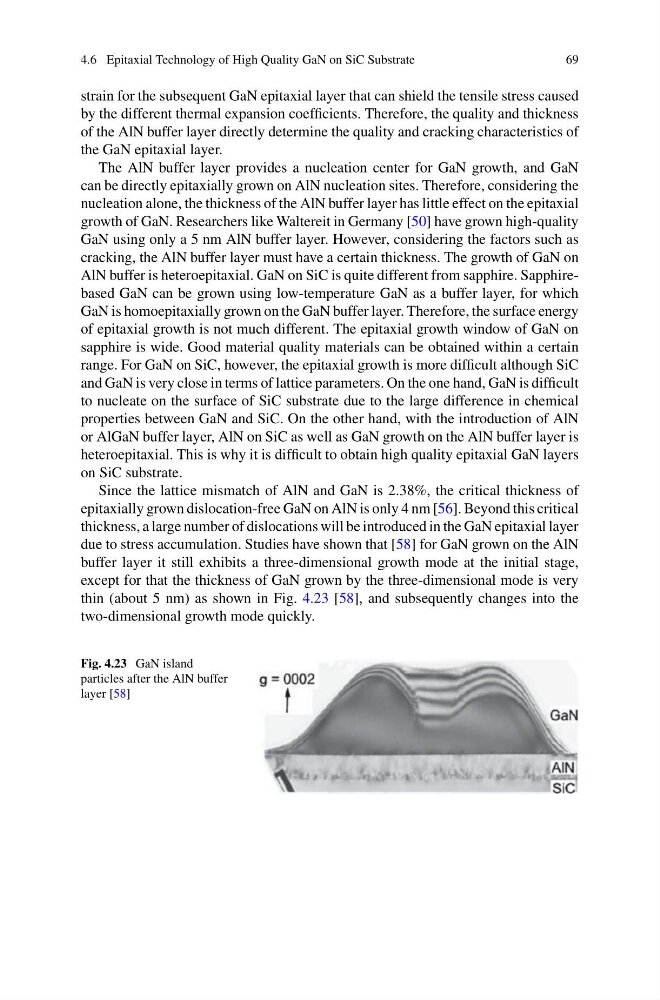
due to stress accumulation. Studies have shown that [58] for GaN grown on the AlN
buffer layer it still exhibits a three-dimensional growth mode at the initial stage,
except for that the thickness of GaN grown by the three-dimensional mode is very
thin (about 5 nm) as shown in Fig. 4.23 [58], and subsequently changes into the
two-dimensional growth mode quickly.
Fig. 4.23 GaN island
particles after the AlN buffer
layer [58]
69
strain for the subsequent GaN epitaxial layer that can shield the tensile stress caused
by the different thermal expansion coefficients. Therefore, the quality and thickness
of the AlN buffer layer directly determine the quality and cracking characteristics of
the GaN epitaxial layer.
The AlN buffer layer provides a nucleation center for GaN growth, and GaN
can be directly epitaxially grown on AlN nucleation sites. Therefore, considering the
nucleation alone, the thickness of the AlN buffer layer has little effect on the epitaxial
growth of GaN. Researchers like Waltereit in Germany [50] have grown high-quality
GaN using only a 5 nm AlN buffer layer. However, considering the factors such as
cracking, the AlN buffer layer must have a certain thickness. The growth of GaN on
AlN buffer is heteroepitaxial. GaN on SiC is quite different from sapphire. Sapphirebased GaN can be grown using low-temperature GaN as a buffer layer, for which
GaN is homoepitaxially grown on the GaN buffer layer. Therefore, the surface energy
of epitaxial growth is not much different. The epitaxial growth window of GaN on
sapphire is wide. Good material quality materials can be obtained within a certain
range. For GaN on SiC, however, the epitaxial growth is more difficult although SiC
and GaN is very close in terms of lattice parameters. On the one hand, GaN is difficult
to nucleate on the surface of SiC substrate due to the large difference in chemical
properties between GaN and SiC. On the other hand, with the introduction of AlN
or AlGaN buffer layer, AlN on SiC as well as GaN growth on the AlN buffer layer is
heteroepitaxial. This is why it is difficult to obtain high quality epitaxial GaN layers
on SiC substrate.
Since the lattice mismatch of AlN and GaN is 2.38%, the critical thickness of
epitaxially grown dislocation-free GaN on AlN is only 4 nm [56]. Beyond this critical
thickness, a large number of dislocations will be introduced in the GaN epitaxial layer
due to stress accumulation. Studies have shown that [58] for GaN grown on the AlN
buffer layer it still exhibits a three-dimensional growth mode at the initial stage,
except for that the thickness of GaN grown by the three-dimensional mode is very
thin (about 5 nm) as shown in Fig. 4.23 [58], and subsequently changes into the
two-dimensional growth mode quickly.
Fig. 4.23 GaN island
particles after the AlN buffer
layer [58]