

60
4 Epitaxial of III-Nitride LED Materials
is increased by a factor of four. This can be explained by the high defect density
caused by the growth mode deviated from lateral growth. The experimental results
are basically consistent with that reported by Lee et al. [33] and Kim et al. [34], but
different from that reported by Juang et al. [35]. The reason for the difference could
be that the Ga flow taken in Juang’s experiment is too small (Ga flow is 4–6 sccm,
corresponding to 20–30 μmol/min).
4.5.1.4 Effect of Buffer Layer Growth Pressure
We conducted a buffer layer experiment with different pressures under the same
Ga flow. The experimental results show that the decrease of pressure will reduce
the migration ability of the reactant atomic groups, and lead to a small and dense
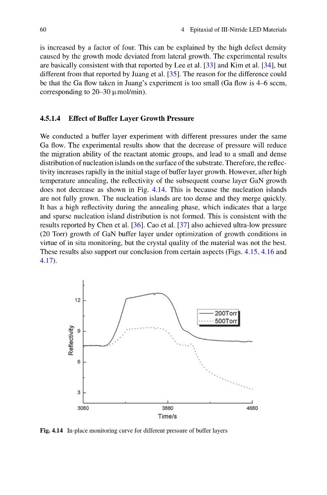
distribution of nucleation islands on the surface of the substrate. Therefore, the reflectivity increases rapidly in the initial stage of buffer layer growth. However, after high
temperature annealing, the reflectivity of the subsequent coarse layer GaN growth
does not decrease as shown in Fig. 4.14. This is because the nucleation islands
are not fully grown. The nucleation islands are too dense and they merge quickly.
It has a high reflectivity during the annealing phase, which indicates that a large
and sparse nucleation island distribution is not formed. This is consistent with the
results reported by Chen et al. [36]. Cao et al. [37] also achieved ultra-low pressure
(20 Torr) growth of GaN buffer layer under optimization of growth conditions in
virtue of in situ monitoring, but the crystal quality of the material was not the best.
These results also support our conclusion from certain aspects (Figs. 4.15, 4.16 and
4.17).
Fig. 4.14 In-place monitoring curve for different pressure of buffer layers
4 Epitaxial of III-Nitride LED Materials
is increased by a factor of four. This can be explained by the high defect density
caused by the growth mode deviated from lateral growth. The experimental results
are basically consistent with that reported by Lee et al. [33] and Kim et al. [34], but
different from that reported by Juang et al. [35]. The reason for the difference could
be that the Ga flow taken in Juang’s experiment is too small (Ga flow is 4–6 sccm,
corresponding to 20–30 μmol/min).
4.5.1.4 Effect of Buffer Layer Growth Pressure
We conducted a buffer layer experiment with different pressures under the same
Ga flow. The experimental results show that the decrease of pressure will reduce
the migration ability of the reactant atomic groups, and lead to a small and dense
distribution of nucleation islands on the surface of the substrate. Therefore, the reflectivity increases rapidly in the initial stage of buffer layer growth. However, after high
temperature annealing, the reflectivity of the subsequent coarse layer GaN growth
does not decrease as shown in Fig. 4.14. This is because the nucleation islands
are not fully grown. The nucleation islands are too dense and they merge quickly.
It has a high reflectivity during the annealing phase, which indicates that a large
and sparse nucleation island distribution is not formed. This is consistent with the
results reported by Chen et al. [36]. Cao et al. [37] also achieved ultra-low pressure
(20 Torr) growth of GaN buffer layer under optimization of growth conditions in
virtue of in situ monitoring, but the crystal quality of the material was not the best.
These results also support our conclusion from certain aspects (Figs. 4.15, 4.16 and
4.17).
Fig. 4.14 In-place monitoring curve for different pressure of buffer layers