

4.5 Influence of Growth Conditions on Epitaxial Layer Quality …
59
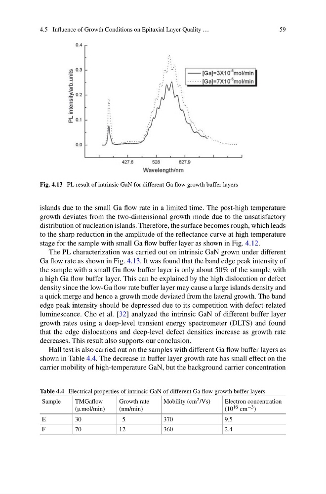
Fig. 4.13 PL result of intrinsic GaN for different Ga flow growth buffer layers
islands due to the small Ga flow rate in a limited time. The post-high temperature
growth deviates from the two-dimensional growth mode due to the unsatisfactory
distribution of nucleation islands. Therefore, the surface becomes rough, which leads
to the sharp reduction in the amplitude of the reflectance curve at high temperature
stage for the sample with small Ga flow buffer layer as shown in Fig. 4.12.
The PL characterization was carried out on intrinsic GaN grown under different
Ga flow rate as shown in Fig. 4.13. It was found that the band edge peak intensity of
the sample with a small Ga flow buffer layer is only about 50% of the sample with
a high Ga flow buffer layer. This can be explained by the high dislocation or defect
density since the low-Ga flow rate buffer layer may cause a large islands density and
a quick merge and hence a growth mode deviated from the lateral growth. The band
edge peak intensity should be depressed due to its competition with defect-related
luminescence. Cho et al. [32] analyzed the intrinsic GaN of different buffer layer
growth rates using a deep-level transient energy spectrometer (DLTS) and found
that the edge dislocations and deep-level defect densities increase as growth rate
decreases. This result also supports our conclusion.
Hall test is also carried out on the samples with different Ga flow buffer layers as
shown in Table 4.4. The decrease in buffer layer growth rate has small effect on the
carrier mobility of high-temperature GaN, but the background carrier concentration
Table 4.4 Electrical properties of intrinsic GaN of different Ga flow growth buffer layers
Sample
TMGaflow
(μmol/min)
Growth rate
(nm/min)
Mobility (cm 2 /Vs)
Electron concentration
(10 16 cm −3 )
E
30
5
370
9.5
F
70
12
360
2.4
59
Fig. 4.13 PL result of intrinsic GaN for different Ga flow growth buffer layers
islands due to the small Ga flow rate in a limited time. The post-high temperature
growth deviates from the two-dimensional growth mode due to the unsatisfactory
distribution of nucleation islands. Therefore, the surface becomes rough, which leads
to the sharp reduction in the amplitude of the reflectance curve at high temperature
stage for the sample with small Ga flow buffer layer as shown in Fig. 4.12.
The PL characterization was carried out on intrinsic GaN grown under different
Ga flow rate as shown in Fig. 4.13. It was found that the band edge peak intensity of
the sample with a small Ga flow buffer layer is only about 50% of the sample with
a high Ga flow buffer layer. This can be explained by the high dislocation or defect
density since the low-Ga flow rate buffer layer may cause a large islands density and
a quick merge and hence a growth mode deviated from the lateral growth. The band
edge peak intensity should be depressed due to its competition with defect-related
luminescence. Cho et al. [32] analyzed the intrinsic GaN of different buffer layer
growth rates using a deep-level transient energy spectrometer (DLTS) and found
that the edge dislocations and deep-level defect densities increase as growth rate
decreases. This result also supports our conclusion.
Hall test is also carried out on the samples with different Ga flow buffer layers as
shown in Table 4.4. The decrease in buffer layer growth rate has small effect on the
carrier mobility of high-temperature GaN, but the background carrier concentration
Table 4.4 Electrical properties of intrinsic GaN of different Ga flow growth buffer layers
Sample
TMGaflow
(μmol/min)
Growth rate
(nm/min)
Mobility (cm 2 /Vs)
Electron concentration
(10 16 cm −3 )
E
30
5
370
9.5
F
70
12
360
2.4