

9.3 LED Packaging Technology
197
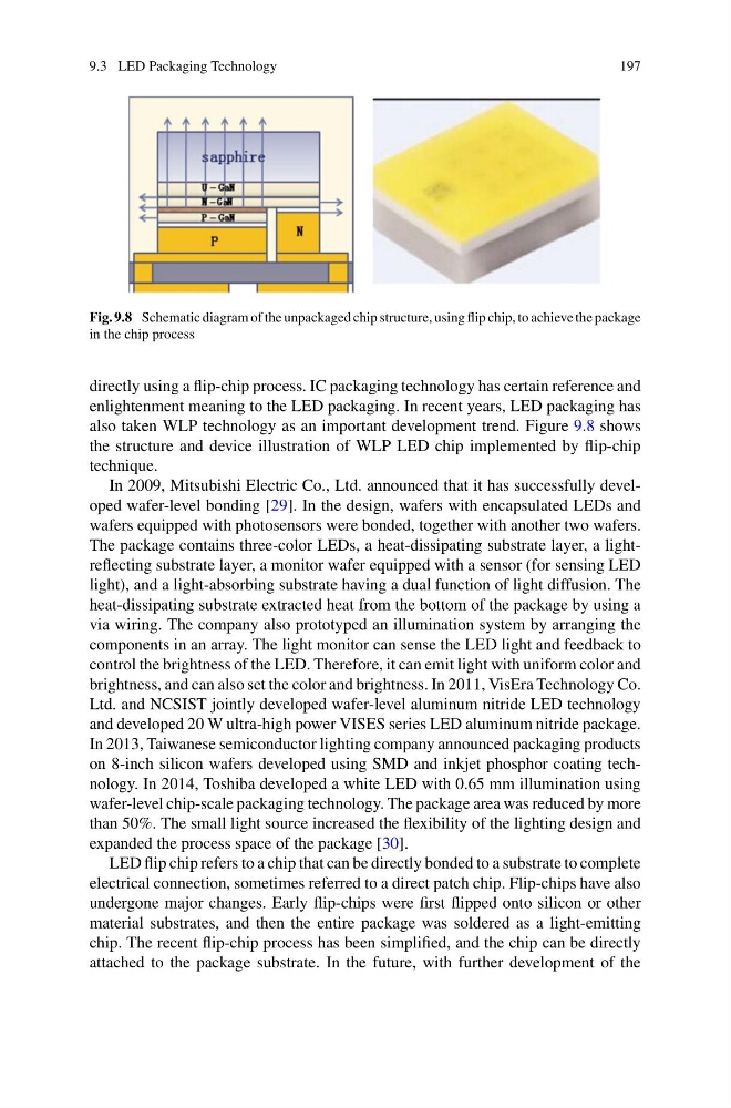
Fig. 9.8 Schematic diagram of the unpackaged chip structure, using flip chip, to achieve the package
in the chip process
directly using a flip-chip process. IC packaging technology has certain reference and
enlightenment meaning to the LED packaging. In recent years, LED packaging has
also taken WLP technology as an important development trend. Figure 9.8 shows
the structure and device illustration of WLP LED chip implemented by flip-chip
technique.
In 2009, Mitsubishi Electric Co., Ltd. announced that it has successfully developed wafer-level bonding [29]. In the design, wafers with encapsulated LEDs and
wafers equipped with photosensors were bonded, together with another two wafers.
The package contains three-color LEDs, a heat-dissipating substrate layer, a lightreflecting substrate layer, a monitor wafer equipped with a sensor (for sensing LED
light), and a light-absorbing substrate having a dual function of light diffusion. The
heat-dissipating substrate extracted heat from the bottom of the package by using a
via wiring. The company also prototyped an illumination system by arranging the
components in an array. The light monitor can sense the LED light and feedback to
control the brightness of the LED. Therefore, it can emit light with uniform color and
brightness, and can also set the color and brightness. In 2011, VisEra Technology Co.
Ltd. and NCSIST jointly developed wafer-level aluminum nitride LED technology
and developed 20 W ultra-high power VISES series LED aluminum nitride package.
In 2013, Taiwanese semiconductor lighting company announced packaging products
on 8-inch silicon wafers developed using SMD and inkjet phosphor coating technology. In 2014, Toshiba developed a white LED with 0.65 mm illumination using
wafer-level chip-scale packaging technology. The package area was reduced by more
than 50%. The small light source increased the flexibility of the lighting design and
expanded the process space of the package [30].
LED flip chip refers to a chip that can be directly bonded to a substrate to complete
electrical connection, sometimes referred to a direct patch chip. Flip-chips have also
undergone major changes. Early flip-chips were first flipped onto silicon or other
material substrates, and then the entire package was soldered as a light-emitting
chip. The recent flip-chip process has been simplified, and the chip can be directly
attached to the package substrate. In the future, with further development of the
197
Fig. 9.8 Schematic diagram of the unpackaged chip structure, using flip chip, to achieve the package
in the chip process
directly using a flip-chip process. IC packaging technology has certain reference and
enlightenment meaning to the LED packaging. In recent years, LED packaging has
also taken WLP technology as an important development trend. Figure 9.8 shows
the structure and device illustration of WLP LED chip implemented by flip-chip
technique.
In 2009, Mitsubishi Electric Co., Ltd. announced that it has successfully developed wafer-level bonding [29]. In the design, wafers with encapsulated LEDs and
wafers equipped with photosensors were bonded, together with another two wafers.
The package contains three-color LEDs, a heat-dissipating substrate layer, a lightreflecting substrate layer, a monitor wafer equipped with a sensor (for sensing LED
light), and a light-absorbing substrate having a dual function of light diffusion. The
heat-dissipating substrate extracted heat from the bottom of the package by using a
via wiring. The company also prototyped an illumination system by arranging the
components in an array. The light monitor can sense the LED light and feedback to
control the brightness of the LED. Therefore, it can emit light with uniform color and
brightness, and can also set the color and brightness. In 2011, VisEra Technology Co.
Ltd. and NCSIST jointly developed wafer-level aluminum nitride LED technology
and developed 20 W ultra-high power VISES series LED aluminum nitride package.
In 2013, Taiwanese semiconductor lighting company announced packaging products
on 8-inch silicon wafers developed using SMD and inkjet phosphor coating technology. In 2014, Toshiba developed a white LED with 0.65 mm illumination using
wafer-level chip-scale packaging technology. The package area was reduced by more
than 50%. The small light source increased the flexibility of the lighting design and
expanded the process space of the package [30].
LED flip chip refers to a chip that can be directly bonded to a substrate to complete
electrical connection, sometimes referred to a direct patch chip. Flip-chips have also
undergone major changes. Early flip-chips were first flipped onto silicon or other
material substrates, and then the entire package was soldered as a light-emitting
chip. The recent flip-chip process has been simplified, and the chip can be directly
attached to the package substrate. In the future, with further development of the