

196
9 Packaging of Group-III Nitride LED
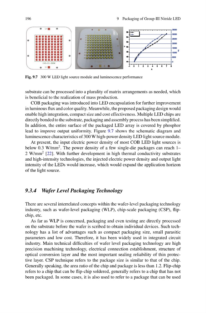
Fig. 9.7 300 W LED light source module and luminescence performance
substrate can be processed into a plurality of matrix arrangements as needed, which
is beneficial to the realization of mass production.
COB packaging was introduced into LED encapsulation for further improvement
in luminous flux and color quality. Meanwhile, the proposed packaging design would
enable high integration, compact size and cost effectiveness. Multiple LED chips are
directly bonded to the substrate, packaging and assembly process has been simplified.
In addition, the entire surface of the packaged LED array is covered by phosphor
lead to improve output uniformity. Figure 9.7 shows the schematic diagram and
luminescence characteristics of 300 W high-power density LED light source module.
At present, the input electric power density of most COB LED light sources is
below 0.3 W/mm
2 . The power density of a few single-die packages can reach 1–
2 W/mm
2 [22]. With further development in high thermal conductivity substrates
and high-intensity technologies, the injected electric power density and output light
intensity of the LEDs would increase, which would expand the application horizon
of the light source.
9.3.4 Wafer Level Packaging Technology
There are several interrelated concepts within the wafer-level packaging technology
industry, such as wafer-level packaging (WLP), chip-scale packaging (CSP), flipchip, etc.
As far as WLP is concerned, packaging and even testing are directly processed
on the substrate before the wafer is scribed to obtain individual devices. Such technology has a list of advantages such as compact packaging size, small parasitic
parameters and low cost. Therefore, it has been widely used in integrated circuit
industry. Main technical difficulties of wafer level packaging technology are high
precision machining technology, electrical connection establishment, structure of
optical conversion layer and the most important sealing reliability of thin protective layer. CSP technique refers to the package size is similar to that of the chip.
Generally speaking, the area ratio of the chip and package is less than 1.2. Flip-chip
refers to a chip that can be flip-chip soldered, generally refers to a chip that has not
been packaged. In some cases, it is also used to refer to a package that can be used
9 Packaging of Group-III Nitride LED
Fig. 9.7 300 W LED light source module and luminescence performance
substrate can be processed into a plurality of matrix arrangements as needed, which
is beneficial to the realization of mass production.
COB packaging was introduced into LED encapsulation for further improvement
in luminous flux and color quality. Meanwhile, the proposed packaging design would
enable high integration, compact size and cost effectiveness. Multiple LED chips are
directly bonded to the substrate, packaging and assembly process has been simplified.
In addition, the entire surface of the packaged LED array is covered by phosphor
lead to improve output uniformity. Figure 9.7 shows the schematic diagram and
luminescence characteristics of 300 W high-power density LED light source module.
At present, the input electric power density of most COB LED light sources is
below 0.3 W/mm
2 . The power density of a few single-die packages can reach 1–
2 W/mm
2 [22]. With further development in high thermal conductivity substrates
and high-intensity technologies, the injected electric power density and output light
intensity of the LEDs would increase, which would expand the application horizon
of the light source.
9.3.4 Wafer Level Packaging Technology
There are several interrelated concepts within the wafer-level packaging technology
industry, such as wafer-level packaging (WLP), chip-scale packaging (CSP), flipchip, etc.
As far as WLP is concerned, packaging and even testing are directly processed
on the substrate before the wafer is scribed to obtain individual devices. Such technology has a list of advantages such as compact packaging size, small parasitic
parameters and low cost. Therefore, it has been widely used in integrated circuit
industry. Main technical difficulties of wafer level packaging technology are high
precision machining technology, electrical connection establishment, structure of
optical conversion layer and the most important sealing reliability of thin protective layer. CSP technique refers to the package size is similar to that of the chip.
Generally speaking, the area ratio of the chip and package is less than 1.2. Flip-chip
refers to a chip that can be flip-chip soldered, generally refers to a chip that has not
been packaged. In some cases, it is also used to refer to a package that can be used