

186
9 Packaging of Group-III Nitride LED
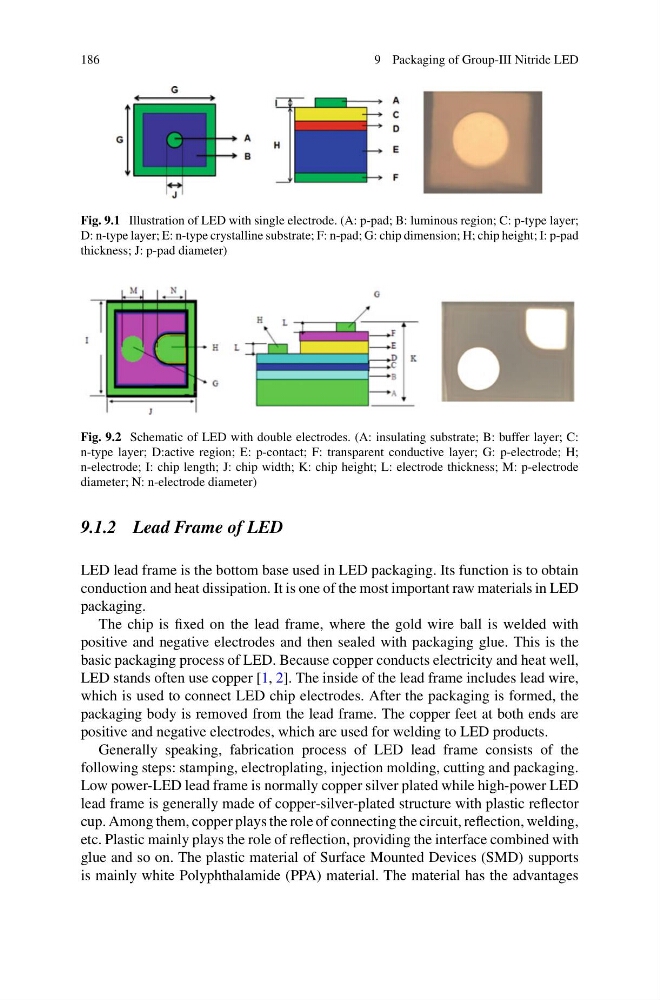
Fig. 9.1 Illustration of LED with single electrode. (A: p-pad; B: luminous region; C: p-type layer;
D: n-type layer; E: n-type crystalline substrate; F: n-pad; G: chip dimension; H; chip height; I: p-pad
thickness; J: p-pad diameter)
Fig. 9.2 Schematic of LED with double electrodes. (A: insulating substrate; B: buffer layer; C:
n-type layer; D:active region; E: p-contact; F: transparent conductive layer; G: p-electrode; H;
n-electrode; I: chip length; J: chip width; K: chip height; L: electrode thickness; M: p-electrode
diameter; N: n-electrode diameter)
9.1.2 Lead Frame of LED
LED lead frame is the bottom base used in LED packaging. Its function is to obtain
conduction and heat dissipation. It is one of the most important raw materials in LED
packaging.
The chip is fixed on the lead frame, where the gold wire ball is welded with
positive and negative electrodes and then sealed with packaging glue. This is the
basic packaging process of LED. Because copper conducts electricity and heat well,
LED stands often use copper [1, 2]. The inside of the lead frame includes lead wire,
which is used to connect LED chip electrodes. After the packaging is formed, the
packaging body is removed from the lead frame. The copper feet at both ends are
positive and negative electrodes, which are used for welding to LED products.
Generally speaking, fabrication process of LED lead frame consists of the
following steps: stamping, electroplating, injection molding, cutting and packaging.
Low power-LED lead frame is normally copper silver plated while high-power LED
lead frame is generally made of copper-silver-plated structure with plastic reflector
cup. Among them, copper plays the role of connecting the circuit, reflection, welding,
etc. Plastic mainly plays the role of reflection, providing the interface combined with
glue and so on. The plastic material of Surface Mounted Devices (SMD) supports
is mainly white Polyphthalamide (PPA) material. The material has the advantages
9 Packaging of Group-III Nitride LED
Fig. 9.1 Illustration of LED with single electrode. (A: p-pad; B: luminous region; C: p-type layer;
D: n-type layer; E: n-type crystalline substrate; F: n-pad; G: chip dimension; H; chip height; I: p-pad
thickness; J: p-pad diameter)
Fig. 9.2 Schematic of LED with double electrodes. (A: insulating substrate; B: buffer layer; C:
n-type layer; D:active region; E: p-contact; F: transparent conductive layer; G: p-electrode; H;
n-electrode; I: chip length; J: chip width; K: chip height; L: electrode thickness; M: p-electrode
diameter; N: n-electrode diameter)
9.1.2 Lead Frame of LED
LED lead frame is the bottom base used in LED packaging. Its function is to obtain
conduction and heat dissipation. It is one of the most important raw materials in LED
packaging.
The chip is fixed on the lead frame, where the gold wire ball is welded with
positive and negative electrodes and then sealed with packaging glue. This is the
basic packaging process of LED. Because copper conducts electricity and heat well,
LED stands often use copper [1, 2]. The inside of the lead frame includes lead wire,
which is used to connect LED chip electrodes. After the packaging is formed, the
packaging body is removed from the lead frame. The copper feet at both ends are
positive and negative electrodes, which are used for welding to LED products.
Generally speaking, fabrication process of LED lead frame consists of the
following steps: stamping, electroplating, injection molding, cutting and packaging.
Low power-LED lead frame is normally copper silver plated while high-power LED
lead frame is generally made of copper-silver-plated structure with plastic reflector
cup. Among them, copper plays the role of connecting the circuit, reflection, welding,
etc. Plastic mainly plays the role of reflection, providing the interface combined with
glue and so on. The plastic material of Surface Mounted Devices (SMD) supports
is mainly white Polyphthalamide (PPA) material. The material has the advantages