

180
8 III-Nitride LED Chip Fabrication Techniques
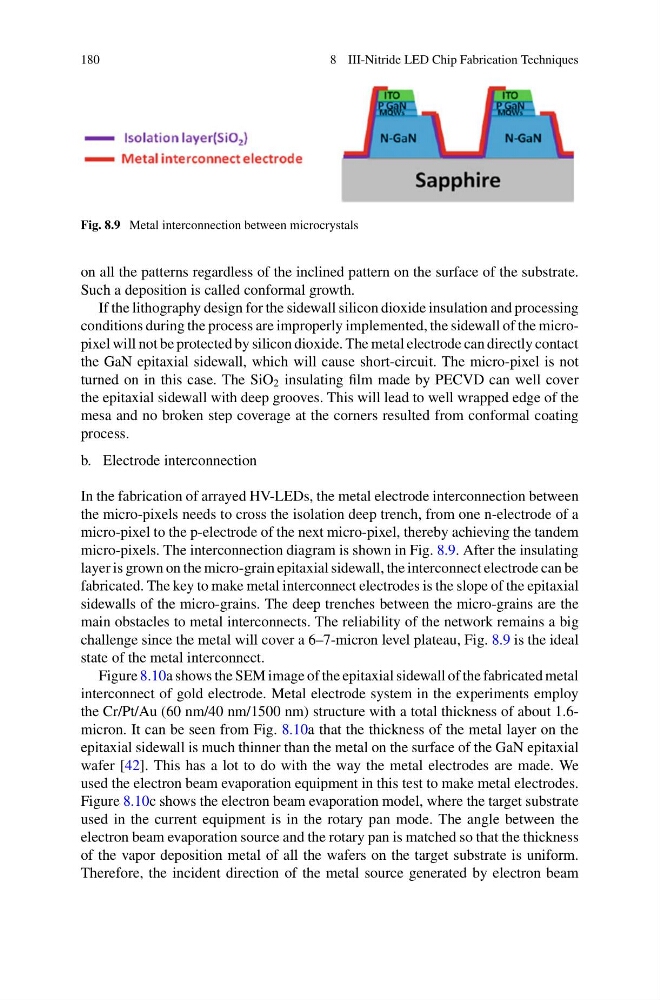
Fig. 8.9 Metal interconnection between microcrystals
on all the patterns regardless of the inclined pattern on the surface of the substrate.
Such a deposition is called conformal growth.
If the lithography design for the sidewall silicon dioxide insulation and processing
conditions during the process are improperly implemented, the sidewall of the micropixel will not be protected by silicon dioxide. The metal electrode can directly contact
the GaN epitaxial sidewall, which will cause short-circuit. The micro-pixel is not
turned on in this case. The SiO 2 insulating film made by PECVD can well cover
the epitaxial sidewall with deep grooves. This will lead to well wrapped edge of the
mesa and no broken step coverage at the corners resulted from conformal coating
process.
b. Electrode interconnection
In the fabrication of arrayed HV-LEDs, the metal electrode interconnection between
the micro-pixels needs to cross the isolation deep trench, from one n-electrode of a
micro-pixel to the p-electrode of the next micro-pixel, thereby achieving the tandem
micro-pixels. The interconnection diagram is shown in Fig. 8.9. After the insulating
layer is grown on the micro-grain epitaxial sidewall, the interconnect electrode can be
fabricated. The key to make metal interconnect electrodes is the slope of the epitaxial
sidewalls of the micro-grains. The deep trenches between the micro-grains are the
main obstacles to metal interconnects. The reliability of the network remains a big
challenge since the metal will cover a 6–7-micron level plateau, Fig. 8.9 is the ideal
state of the metal interconnect.
Figure 8.10a shows the SEM image of the epitaxial sidewall of the fabricated metal
interconnect of gold electrode. Metal electrode system in the experiments employ
the Cr/Pt/Au (60 nm/40 nm/1500 nm) structure with a total thickness of about 1.6micron. It can be seen from Fig. 8.10a that the thickness of the metal layer on the
epitaxial sidewall is much thinner than the metal on the surface of the GaN epitaxial
wafer [42]. This has a lot to do with the way the metal electrodes are made. We
used the electron beam evaporation equipment in this test to make metal electrodes.
Figure 8.10c shows the electron beam evaporation model, where the target substrate
used in the current equipment is in the rotary pan mode. The angle between the
electron beam evaporation source and the rotary pan is matched so that the thickness
of the vapor deposition metal of all the wafers on the target substrate is uniform.
Therefore, the incident direction of the metal source generated by electron beam
8 III-Nitride LED Chip Fabrication Techniques
Fig. 8.9 Metal interconnection between microcrystals
on all the patterns regardless of the inclined pattern on the surface of the substrate.
Such a deposition is called conformal growth.
If the lithography design for the sidewall silicon dioxide insulation and processing
conditions during the process are improperly implemented, the sidewall of the micropixel will not be protected by silicon dioxide. The metal electrode can directly contact
the GaN epitaxial sidewall, which will cause short-circuit. The micro-pixel is not
turned on in this case. The SiO 2 insulating film made by PECVD can well cover
the epitaxial sidewall with deep grooves. This will lead to well wrapped edge of the
mesa and no broken step coverage at the corners resulted from conformal coating
process.
b. Electrode interconnection
In the fabrication of arrayed HV-LEDs, the metal electrode interconnection between
the micro-pixels needs to cross the isolation deep trench, from one n-electrode of a
micro-pixel to the p-electrode of the next micro-pixel, thereby achieving the tandem
micro-pixels. The interconnection diagram is shown in Fig. 8.9. After the insulating
layer is grown on the micro-grain epitaxial sidewall, the interconnect electrode can be
fabricated. The key to make metal interconnect electrodes is the slope of the epitaxial
sidewalls of the micro-grains. The deep trenches between the micro-grains are the
main obstacles to metal interconnects. The reliability of the network remains a big
challenge since the metal will cover a 6–7-micron level plateau, Fig. 8.9 is the ideal
state of the metal interconnect.
Figure 8.10a shows the SEM image of the epitaxial sidewall of the fabricated metal
interconnect of gold electrode. Metal electrode system in the experiments employ
the Cr/Pt/Au (60 nm/40 nm/1500 nm) structure with a total thickness of about 1.6micron. It can be seen from Fig. 8.10a that the thickness of the metal layer on the
epitaxial sidewall is much thinner than the metal on the surface of the GaN epitaxial
wafer [42]. This has a lot to do with the way the metal electrodes are made. We
used the electron beam evaporation equipment in this test to make metal electrodes.
Figure 8.10c shows the electron beam evaporation model, where the target substrate
used in the current equipment is in the rotary pan mode. The angle between the
electron beam evaporation source and the rotary pan is matched so that the thickness
of the vapor deposition metal of all the wafers on the target substrate is uniform.
Therefore, the incident direction of the metal source generated by electron beam