

170
8 III-Nitride LED Chip Fabrication Techniques
Table 8.3 Thermal conductivity of each material of 3 conductive channels
Materials
Sapphire
Silver glue
GaN
Metal alloy
Thermal conductivity [W/(m K)]
35–36
2.5–30
130
>200
conventional wire bonding gold wire shows a tension of about 10 g, while the flip
chips can have a pressure force up to 2000 g. Conventional wire bonding is a point
contact. An instantaneous large current impact can easily melt the wire. On the other
hand, flip chip bonding is a surface contact and can withstand large current surges.
In addition, the conductive traces of the wire bond chip are sapphire, silver paste
and thermally conductive substrate. The thermal conduction channels of the flip chip
solder are GaN, metal bumps and flip-chip substrates. The thermal conductivity of
each material can be seen in Table 8.3. The sapphire and the silver paste have low
thermal conductivity and poor thermal conductivity for the wire bonding structure.
For the flip-chip structure, GaN and metal alloys have high thermal conductivity and
low heat resistance. Such a scheme will provide better heat dissipation performance.
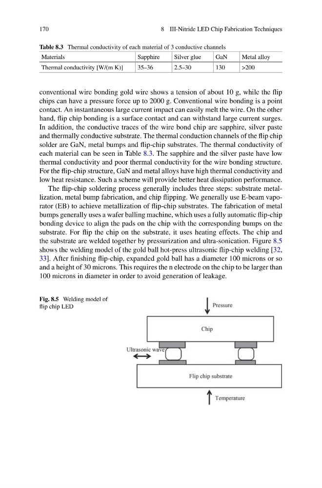
The flip-chip soldering process generally includes three steps: substrate metallization, metal bump fabrication, and chip flipping. We generally use E-beam vaporator (EB) to achieve metallization of flip-chip substrates. The fabrication of metal
bumps generally uses a wafer balling machine, which uses a fully automatic flip-chip
bonding device to align the pads on the chip with the corresponding bumps on the
substrate. For flip the chip on the substrate, it uses heating effects. The chip and
the substrate are welded together by pressurization and ultra-sonication. Figure 8.5
shows the welding model of the gold ball hot-press ultrasonic flip-chip welding [32,
33]. After finishing flip-chip, expanded gold ball has a diameter 100 microns or so
and a height of 30 microns. This requires the n electrode on the chip to be larger than
100 microns in diameter in order to avoid generation of leakage.
Fig. 8.5 Welding model of
flip chip LED
8 III-Nitride LED Chip Fabrication Techniques
Table 8.3 Thermal conductivity of each material of 3 conductive channels
Materials
Sapphire
Silver glue
GaN
Metal alloy
Thermal conductivity [W/(m K)]
35–36
2.5–30
130
>200
conventional wire bonding gold wire shows a tension of about 10 g, while the flip
chips can have a pressure force up to 2000 g. Conventional wire bonding is a point
contact. An instantaneous large current impact can easily melt the wire. On the other
hand, flip chip bonding is a surface contact and can withstand large current surges.
In addition, the conductive traces of the wire bond chip are sapphire, silver paste
and thermally conductive substrate. The thermal conduction channels of the flip chip
solder are GaN, metal bumps and flip-chip substrates. The thermal conductivity of
each material can be seen in Table 8.3. The sapphire and the silver paste have low
thermal conductivity and poor thermal conductivity for the wire bonding structure.
For the flip-chip structure, GaN and metal alloys have high thermal conductivity and
low heat resistance. Such a scheme will provide better heat dissipation performance.
The flip-chip soldering process generally includes three steps: substrate metallization, metal bump fabrication, and chip flipping. We generally use E-beam vaporator (EB) to achieve metallization of flip-chip substrates. The fabrication of metal
bumps generally uses a wafer balling machine, which uses a fully automatic flip-chip
bonding device to align the pads on the chip with the corresponding bumps on the
substrate. For flip the chip on the substrate, it uses heating effects. The chip and
the substrate are welded together by pressurization and ultra-sonication. Figure 8.5
shows the welding model of the gold ball hot-press ultrasonic flip-chip welding [32,
33]. After finishing flip-chip, expanded gold ball has a diameter 100 microns or so
and a height of 30 microns. This requires the n electrode on the chip to be larger than
100 microns in diameter in order to avoid generation of leakage.
Fig. 8.5 Welding model of
flip chip LED