

154
8 III-Nitride LED Chip Fabrication Techniques
Positive photoresist, after exposing to UV light, becomes soluble in the developing
solution. The positive gel is generally composed of a novella resin polymer. The
cross-linked light sensitizer contained in the resin can decompose the sensitizer and
break the cross-linking chemical bond, thereby becoming soluble in the developer.
The unexposed positive photoresist is in-soluble in the developer. In other words,
the pattern after exposing and developing will be the same as the mask pattern. Due
to the lack of expansion, positive photoresist generally achieves higher resolution in
LED manufacturing as well as in traditional IC manufacturing applications.
8.2.2 Lithography Process
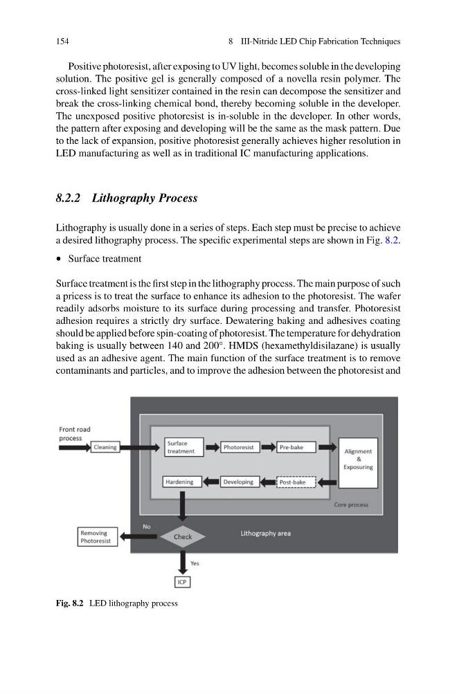
Lithography is usually done in a series of steps. Each step must be precise to achieve
a desired lithography process. The specific experimental steps are shown in Fig. 8.2.
• Surface treatment
Surface treatment is the first step in the lithography process. The main purpose of such
a pricess is to treat the surface to enhance its adhesion to the photoresist. The wafer
readily adsorbs moisture to its surface during processing and transfer. Photoresist
adhesion requires a strictly dry surface. Dewatering baking and adhesives coating
should be applied before spin-coating of photoresist. The temperature for dehydration
baking is usually between 140 and 200°. HMDS (hexamethyldisilazane) is usually
used as an adhesive agent. The main function of the surface treatment is to remove
contaminants and particles, and to improve the adhesion between the photoresist and
Fig. 8.2 LED lithography process
8 III-Nitride LED Chip Fabrication Techniques
Positive photoresist, after exposing to UV light, becomes soluble in the developing
solution. The positive gel is generally composed of a novella resin polymer. The
cross-linked light sensitizer contained in the resin can decompose the sensitizer and
break the cross-linking chemical bond, thereby becoming soluble in the developer.
The unexposed positive photoresist is in-soluble in the developer. In other words,
the pattern after exposing and developing will be the same as the mask pattern. Due
to the lack of expansion, positive photoresist generally achieves higher resolution in
LED manufacturing as well as in traditional IC manufacturing applications.
8.2.2 Lithography Process
Lithography is usually done in a series of steps. Each step must be precise to achieve
a desired lithography process. The specific experimental steps are shown in Fig. 8.2.
• Surface treatment
Surface treatment is the first step in the lithography process. The main purpose of such
a pricess is to treat the surface to enhance its adhesion to the photoresist. The wafer
readily adsorbs moisture to its surface during processing and transfer. Photoresist
adhesion requires a strictly dry surface. Dewatering baking and adhesives coating
should be applied before spin-coating of photoresist. The temperature for dehydration
baking is usually between 140 and 200°. HMDS (hexamethyldisilazane) is usually
used as an adhesive agent. The main function of the surface treatment is to remove
contaminants and particles, and to improve the adhesion between the photoresist and
Fig. 8.2 LED lithography process