

8.2 Photolithography
153
the lithography process. All operations in the lithography process are based on the
specific photoresist properties and fine-tuning. The design of the photomasks, the
selection of the photoresists and the development of the lithography process are a
very long process. A complete and mature lithography process needs to be continuously optimized and adjusted. The lithography process is important in the LED
fabrication.
8.2.1 Mask and Photoresist
First, the photolithography process requires the wafer to be as close as possible
to the design patterns. The graphics of this design are realized by the photomasks
containing all the elements from the pattern layout, so the lithographic quality of the
photomasks plays a very important role in the lithography process. The pattern with
photomasks is the one will be eventually implemented on the wafer surface. Usually
LED wafer fabrication process includes multiple photolithography processes. The
device pattern on the LED wafer is typically established by a number of specific
masks.
Photoresist is a light-sensitive organic compound composed of a photosensitive
resin, a sensitizer and a solvent. When such a photosensitive material is subject to
the UV exposure, the solubility of the photoresist in the developing solution will
change accordingly. The photoresist used in device fabrication is usually applied to
the surface of a silicon wafer in a liquid state and then dried to be a gel-like film.
According to the chemical reaction mechanism and development principle of the
photoresist, it can be divided into a positive photoresist and a negative photoresist. Negative photoresist is used in the early development of lithography process.
Its process cost is low and the output is high. However, since it will expand after
absorbing the developer, its resolution is not as good as that of positive photoresist.
Therefore, for sub-micron or even smaller size, positive photoresist is most widely
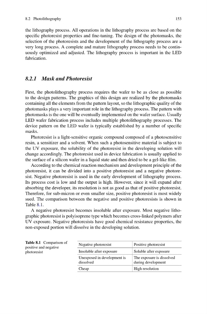
sued. The comparison between the negative and positive photoresists is shown in
Table 8.1.
A negative photoresist becomes insoluble after exposure. Most negative lithographic photoresist is polyisoprene type which becomes cross-linked polymers after
UV exposure. Negative photoresists have good chemical resistance properties, the
non-exposed portion will dissolve in the developing solution.
Table 8.1 Comparison of
positive and negative
photoresist
Negative photoresist
Positive photoresist
Insoluble after exposure
Soluble after exposure
Unexposed in development is
dissolved
The exposure is dissolved
during development
Cheap
High resolution
153
the lithography process. All operations in the lithography process are based on the
specific photoresist properties and fine-tuning. The design of the photomasks, the
selection of the photoresists and the development of the lithography process are a
very long process. A complete and mature lithography process needs to be continuously optimized and adjusted. The lithography process is important in the LED
fabrication.
8.2.1 Mask and Photoresist
First, the photolithography process requires the wafer to be as close as possible
to the design patterns. The graphics of this design are realized by the photomasks
containing all the elements from the pattern layout, so the lithographic quality of the
photomasks plays a very important role in the lithography process. The pattern with
photomasks is the one will be eventually implemented on the wafer surface. Usually
LED wafer fabrication process includes multiple photolithography processes. The
device pattern on the LED wafer is typically established by a number of specific
masks.
Photoresist is a light-sensitive organic compound composed of a photosensitive
resin, a sensitizer and a solvent. When such a photosensitive material is subject to
the UV exposure, the solubility of the photoresist in the developing solution will
change accordingly. The photoresist used in device fabrication is usually applied to
the surface of a silicon wafer in a liquid state and then dried to be a gel-like film.
According to the chemical reaction mechanism and development principle of the
photoresist, it can be divided into a positive photoresist and a negative photoresist. Negative photoresist is used in the early development of lithography process.
Its process cost is low and the output is high. However, since it will expand after
absorbing the developer, its resolution is not as good as that of positive photoresist.
Therefore, for sub-micron or even smaller size, positive photoresist is most widely
sued. The comparison between the negative and positive photoresists is shown in
Table 8.1.
A negative photoresist becomes insoluble after exposure. Most negative lithographic photoresist is polyisoprene type which becomes cross-linked polymers after
UV exposure. Negative photoresists have good chemical resistance properties, the
non-exposed portion will dissolve in the developing solution.
Table 8.1 Comparison of
positive and negative
photoresist
Negative photoresist
Positive photoresist
Insoluble after exposure
Soluble after exposure
Unexposed in development is
dissolved
The exposure is dissolved
during development
Cheap
High resolution