

7.2 Internal Quantum Efficiency Improvement Technology
123
Fig. 7.8 Schematic diagram
of the carrier recombination
process in InGaN MQWs
well and p-GaN layer. However, this EBL blocks hole injection into the multiple
quantum well region due to its higher valence band barrier. The bending of interface
band due to the piezoelectric polarization field induced by lattice mismatch at the
AlGaN/GaN interface further blocks the injection of holes. In order to eliminate
the stress mismatch between the electron blocking layer and the active region, we
replaced the traditional electron blocking layer (CEBL) with an electron blocking
layer (GEBL) with a gradual increase in composition along the growth direction.
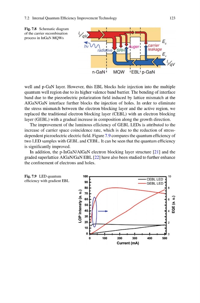
The improvement of the luminous efficiency of GEBL LEDs is attributed to the
increase of carrier space coincidence rate, which is due to the reduction of stressdependent piezoelectric electric field. Figure 7.9 compares the quantum efficiency of
two LED samples with GEBL and CEBL. It can be seen that the quantum efficiency
is significantly improved.
In addition, the p-InGaN/AlGaN electron blocking layer structure [21] and the
graded superlattice AlGaN/GaN EBL [22] have also been studied to further enhance
the confinement of electrons and holes.
Fig. 7.9 LED quantum
efficiency with gradient EBL
123
Fig. 7.8 Schematic diagram
of the carrier recombination
process in InGaN MQWs
well and p-GaN layer. However, this EBL blocks hole injection into the multiple
quantum well region due to its higher valence band barrier. The bending of interface
band due to the piezoelectric polarization field induced by lattice mismatch at the
AlGaN/GaN interface further blocks the injection of holes. In order to eliminate
the stress mismatch between the electron blocking layer and the active region, we
replaced the traditional electron blocking layer (CEBL) with an electron blocking
layer (GEBL) with a gradual increase in composition along the growth direction.
The improvement of the luminous efficiency of GEBL LEDs is attributed to the
increase of carrier space coincidence rate, which is due to the reduction of stressdependent piezoelectric electric field. Figure 7.9 compares the quantum efficiency of
two LED samples with GEBL and CEBL. It can be seen that the quantum efficiency
is significantly improved.
In addition, the p-InGaN/AlGaN electron blocking layer structure [21] and the
graded superlattice AlGaN/GaN EBL [22] have also been studied to further enhance
the confinement of electrons and holes.
Fig. 7.9 LED quantum
efficiency with gradient EBL