

70
G. C. Ghivela et al.
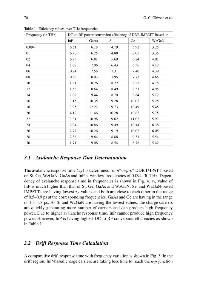
Table 1 Efficiency values over THz frequencies
Frequency (in THz)
DC-to-RF power conversion efficiency of DDR IMPATT based on
InP
GaAs
Si
Ge
WzGaN
0.094
6.51
6.18
4.79
5.92
3.25
01
6.70
6.25
4.88
6.05
3.35
02
6.75
6.81
5.69
6.24
4.01
04
8.68
7.06
6.43
6.36
4.12
06
10.24
7.58
7.31
7.40
4.39
08
10.86
8.03
7.95
7.73
4.65
10
11.21
8.26
8.22
8.25
4.75
12
11.53
8.64
8.49
8.51
4.95
14
12.02
9.44
8.70
8.84
5.12
16
13.15
10.35
9.28
10.02
5.25
18
13.95
12.22
9.73
10.49
5.45
20
14.12
11.46
10.28
10.62
5.75
22
13.31
10.98
9.62
11.02
5.97
24
12.94
10.86
9.49
10.44
6.38
26
12.77
10.26
9.19
10.02
6.05
28
12.36
9.64
8.88
9.31
5.54
30
11.71
9.08
8.54
8.78
5.42
3.1 Avalanche Response Time Determination
The avalanche response time (τ A ) is determined for n
+ -n-p-p
+ DDR IMPATT based
on Si, Ge, WzGaN, GaAs and InP at window frequencies of 0.094–30 THz. Dependency of avalanche response time in frequencies is shown in Fig. 4. τ A value of
InP is much higher than that of Si, Ge, GaAs and WzGaN. Si- and WzGaN-based
IMPATTs are having lowest τ A values and both are close to each other in the range
of 0.5–0.9 ps at the corresponding frequencies. GaAs and Ge are having in the range
of 1.3–1.8 ps. As Si and WzGaN are having the lowest values, the charge carriers
are quickly generating more number of carriers and can produce high frequency
power. Due to higher avalanche response time, InP cannot produce high frequency
power. However, InP is having highest DC-to-RF conversion efficiencies as shown
in Table 1.
3.2 Drift Response Time Calculation
A comparative drift response time with frequency variation is shown in Fig. 5. In the
drift region, InP-based charge carriers are taking less time to reach the n-p junction
G. C. Ghivela et al.
Table 1 Efficiency values over THz frequencies
Frequency (in THz)
DC-to-RF power conversion efficiency of DDR IMPATT based on
InP
GaAs
Si
Ge
WzGaN
0.094
6.51
6.18
4.79
5.92
3.25
01
6.70
6.25
4.88
6.05
3.35
02
6.75
6.81
5.69
6.24
4.01
04
8.68
7.06
6.43
6.36
4.12
06
10.24
7.58
7.31
7.40
4.39
08
10.86
8.03
7.95
7.73
4.65
10
11.21
8.26
8.22
8.25
4.75
12
11.53
8.64
8.49
8.51
4.95
14
12.02
9.44
8.70
8.84
5.12
16
13.15
10.35
9.28
10.02
5.25
18
13.95
12.22
9.73
10.49
5.45
20
14.12
11.46
10.28
10.62
5.75
22
13.31
10.98
9.62
11.02
5.97
24
12.94
10.86
9.49
10.44
6.38
26
12.77
10.26
9.19
10.02
6.05
28
12.36
9.64
8.88
9.31
5.54
30
11.71
9.08
8.54
8.78
5.42
3.1 Avalanche Response Time Determination
The avalanche response time (τ A ) is determined for n
+ -n-p-p
+ DDR IMPATT based
on Si, Ge, WzGaN, GaAs and InP at window frequencies of 0.094–30 THz. Dependency of avalanche response time in frequencies is shown in Fig. 4. τ A value of
InP is much higher than that of Si, Ge, GaAs and WzGaN. Si- and WzGaN-based
IMPATTs are having lowest τ A values and both are close to each other in the range
of 0.5–0.9 ps at the corresponding frequencies. GaAs and Ge are having in the range
of 1.3–1.8 ps. As Si and WzGaN are having the lowest values, the charge carriers
are quickly generating more number of carriers and can produce high frequency
power. Due to higher avalanche response time, InP cannot produce high frequency
power. However, InP is having highest DC-to-RF conversion efficiencies as shown
in Table 1.
3.2 Drift Response Time Calculation
A comparative drift response time with frequency variation is shown in Fig. 5. In the
drift region, InP-based charge carriers are taking less time to reach the n-p junction