

Potentiality of Impact Avalanche Transit Time Diode …
67
where E(x) and q are electric field profile and electronic charge, ε = ε 0 ε s is permittivity of semiconductor, N D and N A are donor and acceptor densities, n and p for
electron and hole, and J and α are current density and ionization rate [14].
2 Numerical Method and Design Parameters
To find the conversion efficiency, the numerical method is initiated from X 0 with E m .
E m and X 0 are initially chosen suitably for the fitted doping profile and current density.
Then, Eqs. (1) and (2) are solved simultaneously by taking space steps of very small
width (0.001 nm). Iteration over E m and X 0 is carried out till boundary conditions
are being satisfied at x = 0 and W. Thus, electric field and current distribution are
obtained from the computations. The method described above gives the avalanche
breakdown characteristics and the avalanche layer width X A . Computer simulation
using MATLAB is carried out, and the width of the epilayers is accordingly chosen
using the transit time formula, W n,p = ((0.5 × V ns,ps )/f ) with π transit angle, where
V s and f are saturation velocity and frequency [17]. The breakdown voltage (V B )
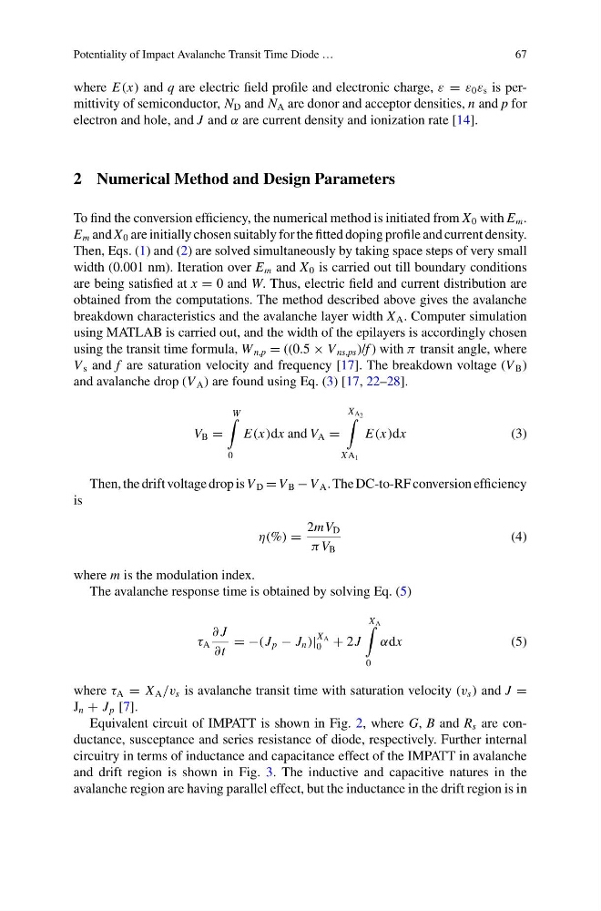
and avalanche drop (V A ) are found using Eq. (3) [17, 22–28].
V B =
W
0
E(x)dx and V A =
X A 2
X A 1
E(x)dx
(3)
Then, the drift voltage drop is V D = V B − V A . The DC-to-RF conversion efficiency
is
η(%) =
2mV D
π V B
(4)
where m is the modulation index.
The avalanche response time is obtained by solving Eq. (5)
τ A
∂ J
∂t
= −(J p − J n )|
X A
0 + 2J
X A
0
αdx
(5)
where τ A = X A /v s is avalanche transit time with saturation velocity (v s ) and J =
J n + J p [7].
Equivalent circuit of IMPATT is shown in Fig. 2, where G, B and R s are conductance, susceptance and series resistance of diode, respectively. Further internal
circuitry in terms of inductance and capacitance effect of the IMPATT in avalanche
and drift region is shown in Fig. 3. The inductive and capacitive natures in the
avalanche region are having parallel effect, but the inductance in the drift region is in
67
where E(x) and q are electric field profile and electronic charge, ε = ε 0 ε s is permittivity of semiconductor, N D and N A are donor and acceptor densities, n and p for
electron and hole, and J and α are current density and ionization rate [14].
2 Numerical Method and Design Parameters
To find the conversion efficiency, the numerical method is initiated from X 0 with E m .
E m and X 0 are initially chosen suitably for the fitted doping profile and current density.
Then, Eqs. (1) and (2) are solved simultaneously by taking space steps of very small
width (0.001 nm). Iteration over E m and X 0 is carried out till boundary conditions
are being satisfied at x = 0 and W. Thus, electric field and current distribution are
obtained from the computations. The method described above gives the avalanche
breakdown characteristics and the avalanche layer width X A . Computer simulation
using MATLAB is carried out, and the width of the epilayers is accordingly chosen
using the transit time formula, W n,p = ((0.5 × V ns,ps )/f ) with π transit angle, where
V s and f are saturation velocity and frequency [17]. The breakdown voltage (V B )
and avalanche drop (V A ) are found using Eq. (3) [17, 22–28].
V B =
W
0
E(x)dx and V A =
X A 2
X A 1
E(x)dx
(3)
Then, the drift voltage drop is V D = V B − V A . The DC-to-RF conversion efficiency
is
η(%) =
2mV D
π V B
(4)
where m is the modulation index.
The avalanche response time is obtained by solving Eq. (5)
τ A
∂ J
∂t
= −(J p − J n )|
X A
0 + 2J
X A
0
αdx
(5)
where τ A = X A /v s is avalanche transit time with saturation velocity (v s ) and J =
J n + J p [7].
Equivalent circuit of IMPATT is shown in Fig. 2, where G, B and R s are conductance, susceptance and series resistance of diode, respectively. Further internal
circuitry in terms of inductance and capacitance effect of the IMPATT in avalanche
and drift region is shown in Fig. 3. The inductive and capacitive natures in the
avalanche region are having parallel effect, but the inductance in the drift region is in