

66
G. C. Ghivela et al.
material [13]. Therefore, here, we have taken Si, Ge, GaAs, InP and WzGaN as
base substrate material to study the conversion efficiency and the delay amount.
Under actual operating condition, considerable amount of DC current flow through
the diode and the space charges modifies the electric field distribution which in turn
affects the current density profiles of electrons and holes by changing the magnitude
of ionization rates. So, through simultaneous solution of the Poisson and current
continuity equations (Eqs. 1 and 2) [14–18], using the computer simulation program,
we can accurately investigate the conversion efficiency, delay amount, inductancecapacitance values in avalanche region and resonant frequencies of IMPATT diode.
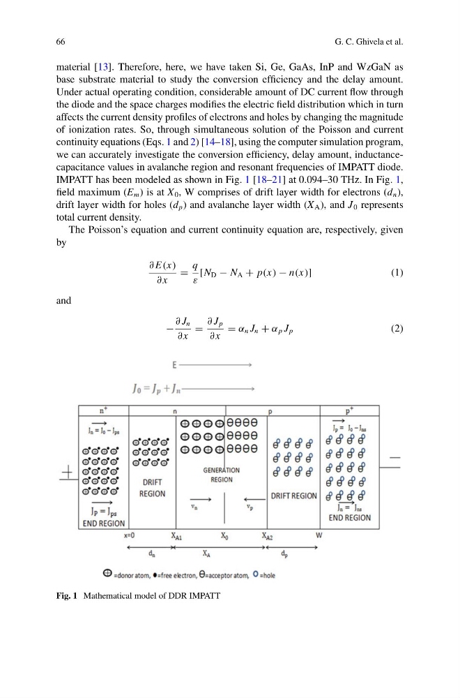
IMPATT has been modeled as shown in Fig. 1 [18–21] at 0.094–30 THz. In Fig. 1,
field maximum (E m ) is at X 0 , W comprises of drift layer width for electrons (d n ),
drift layer width for holes (d p ) and avalanche layer width (X A ), and J 0 represents
total current density.
The Poisson’s equation and current continuity equation are, respectively, given
by
∂ E(x)
∂ x
=
q
ε
[N D − N A + p(x) − n(x)]
(1)
and
−
∂ J n
∂ x
=
∂ J p
∂ x
= α n J n + α p J p
(2)
Fig. 1 Mathematical model of DDR IMPATT
G. C. Ghivela et al.
material [13]. Therefore, here, we have taken Si, Ge, GaAs, InP and WzGaN as
base substrate material to study the conversion efficiency and the delay amount.
Under actual operating condition, considerable amount of DC current flow through
the diode and the space charges modifies the electric field distribution which in turn
affects the current density profiles of electrons and holes by changing the magnitude
of ionization rates. So, through simultaneous solution of the Poisson and current
continuity equations (Eqs. 1 and 2) [14–18], using the computer simulation program,
we can accurately investigate the conversion efficiency, delay amount, inductancecapacitance values in avalanche region and resonant frequencies of IMPATT diode.
IMPATT has been modeled as shown in Fig. 1 [18–21] at 0.094–30 THz. In Fig. 1,
field maximum (E m ) is at X 0 , W comprises of drift layer width for electrons (d n ),
drift layer width for holes (d p ) and avalanche layer width (X A ), and J 0 represents
total current density.
The Poisson’s equation and current continuity equation are, respectively, given
by
∂ E(x)
∂ x
=
q
ε
[N D − N A + p(x) − n(x)]
(1)
and
−
∂ J n
∂ x
=
∂ J p
∂ x
= α n J n + α p J p
(2)
Fig. 1 Mathematical model of DDR IMPATT