

50
R. Singh et al.
Keywords Ultra-wideband gap · Gallium nitride · Gallium oxide · RF
performance · Terahertz · Imaging · Spectroscopy · Bandwidth · High electron
mobility transistor · HEMT
1 Introduction
Outstanding material parameters of ultra-wideband gap (UWG) semiconductors have
provided a solid platform for conclusive research and rapid development of RF
power device applications. With advent of Internet-of-Everything (IoE), systematic
connection of data, things, processes and people, recent time witnessed an upsurge
in high-speed wireless communication market, which has further fuelled demand for
next-generation power devices: high-efficiency power converters, power amplifiers,
and many more. Furthermore, quest for sustainable renewable energy systems and
adoption of electric-vehicles (EV) have pushed additional demand of the powerefficient electronic devices, employing Ga 2 O 3 -, GaN-, and SiC-based transistors
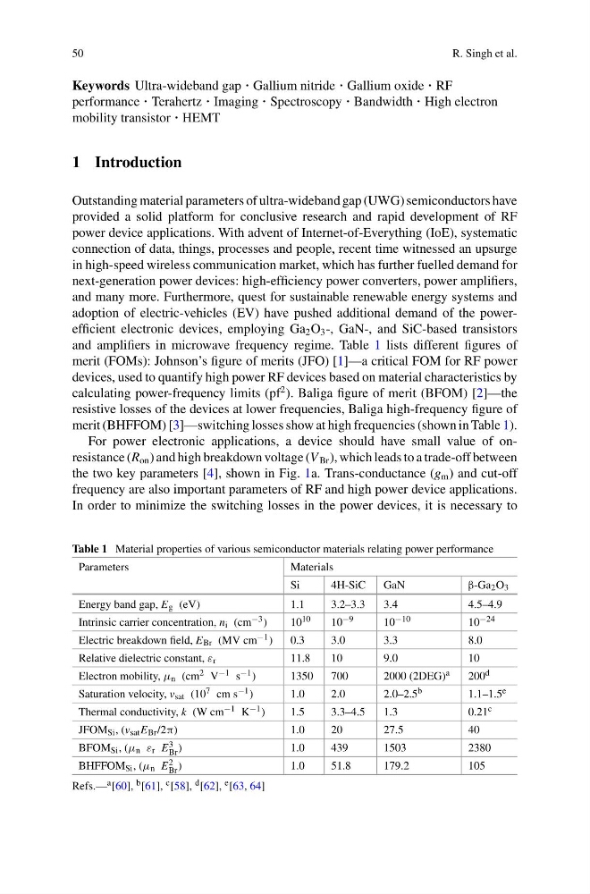
and amplifiers in microwave frequency regime. Table 1 lists different figures of
merit (FOMs): Johnson’s figure of merits (JFO) [1]—a critical FOM for RF power
devices, used to quantify high power RF devices based on material characteristics by
calculating power-frequency limits (pf
2 ). Baliga figure of merit (BFOM) [2]—the
resistive losses of the devices at lower frequencies, Baliga high-frequency figure of
merit (BHFFOM) [3]—switching losses show at high frequencies (shown in Table 1).
For power electronic applications, a device should have small value of onresistance (R on ) and high breakdown voltage (V Br ), which leads to a trade-off between
the two key parameters [4], shown in Fig. 1a. Trans-conductance (g m ) and cut-off
frequency are also important parameters of RF and high power device applications.
In order to minimize the switching losses in the power devices, it is necessary to
Table 1 Material properties of various semiconductor materials relating power performance
Parameters
Materials
Si
4H-SiC
GaN
β-Ga 2 O 3
Energy band gap, E g (eV)
1.1
3.2–3.3
3.4
4.5–4.9
Intrinsic carrier concentration, n i (cm −3 )
10 10
10 −9
10 −10
10 −24
Electric breakdown field, E Br (MV cm −1 )
0.3
3.0
3.3
8.0
Relative dielectric constant, ε r
11.8
10
9.0
10
Electron mobility, μ n (cm 2 V −1 s −1 )
1350
700
2000 (2DEG) a
200 d
Saturation velocity, v sat (10 7 cm s −1 )
1.0
2.0
2.0–2.5 b
1.1–1.5 e
Thermal conductivity, k (W cm −1 K −1 )
1.5
3.3–4.5
1.3
0.21 c
JFOM Si , (v sat E Br /2π)
1.0
20
27.5
40
BFOM Si , (μ n ε r E 3
Br )
1.0
439
1503
2380
BHFFOM Si , (μ n E 2
Br )
1.0
51.8
179.2
105
Refs.— a [60], b [61], c [58], d [62], e [63, 64]
R. Singh et al.
Keywords Ultra-wideband gap · Gallium nitride · Gallium oxide · RF
performance · Terahertz · Imaging · Spectroscopy · Bandwidth · High electron
mobility transistor · HEMT
1 Introduction
Outstanding material parameters of ultra-wideband gap (UWG) semiconductors have
provided a solid platform for conclusive research and rapid development of RF
power device applications. With advent of Internet-of-Everything (IoE), systematic
connection of data, things, processes and people, recent time witnessed an upsurge
in high-speed wireless communication market, which has further fuelled demand for
next-generation power devices: high-efficiency power converters, power amplifiers,
and many more. Furthermore, quest for sustainable renewable energy systems and
adoption of electric-vehicles (EV) have pushed additional demand of the powerefficient electronic devices, employing Ga 2 O 3 -, GaN-, and SiC-based transistors
and amplifiers in microwave frequency regime. Table 1 lists different figures of
merit (FOMs): Johnson’s figure of merits (JFO) [1]—a critical FOM for RF power
devices, used to quantify high power RF devices based on material characteristics by
calculating power-frequency limits (pf
2 ). Baliga figure of merit (BFOM) [2]—the
resistive losses of the devices at lower frequencies, Baliga high-frequency figure of
merit (BHFFOM) [3]—switching losses show at high frequencies (shown in Table 1).
For power electronic applications, a device should have small value of onresistance (R on ) and high breakdown voltage (V Br ), which leads to a trade-off between
the two key parameters [4], shown in Fig. 1a. Trans-conductance (g m ) and cut-off
frequency are also important parameters of RF and high power device applications.
In order to minimize the switching losses in the power devices, it is necessary to
Table 1 Material properties of various semiconductor materials relating power performance
Parameters
Materials
Si
4H-SiC
GaN
β-Ga 2 O 3
Energy band gap, E g (eV)
1.1
3.2–3.3
3.4
4.5–4.9
Intrinsic carrier concentration, n i (cm −3 )
10 10
10 −9
10 −10
10 −24
Electric breakdown field, E Br (MV cm −1 )
0.3
3.0
3.3
8.0
Relative dielectric constant, ε r
11.8
10
9.0
10
Electron mobility, μ n (cm 2 V −1 s −1 )
1350
700
2000 (2DEG) a
200 d
Saturation velocity, v sat (10 7 cm s −1 )
1.0
2.0
2.0–2.5 b
1.1–1.5 e
Thermal conductivity, k (W cm −1 K −1 )
1.5
3.3–4.5
1.3
0.21 c
JFOM Si , (v sat E Br /2π)
1.0
20
27.5
40
BFOM Si , (μ n ε r E 3
Br )
1.0
439
1503
2380
BHFFOM Si , (μ n E 2
Br )
1.0
51.8
179.2
105
Refs.— a [60], b [61], c [58], d [62], e [63, 64]