

590
K. Tawa et al.
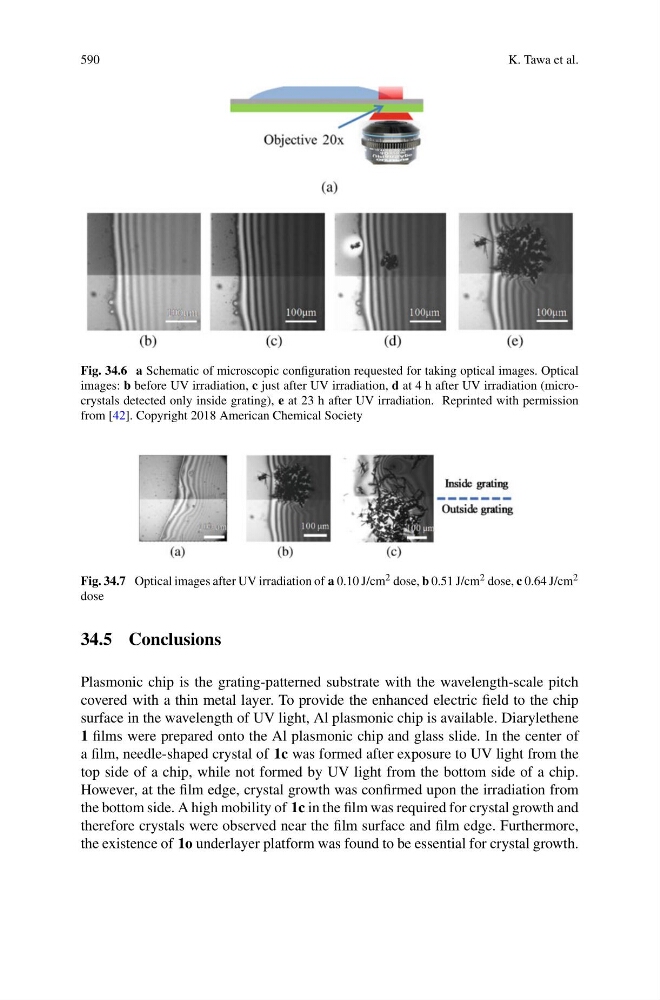
Fig. 34.6 a Schematic of microscopic configuration requested for taking optical images. Optical
images: b before UV irradiation, c just after UV irradiation, d at 4 h after UV irradiation (microcrystals detected only inside grating), e at 23 h after UV irradiation. Reprinted with permission
from [42]. Copyright 2018 American Chemical Society
Fig. 34.7 Optical images after UV irradiation of a 0.10 J/cm 2 dose, b 0.51 J/cm 2 dose, c 0.64 J/cm 2
dose
34.5 Conclusions
Plasmonic chip is the grating-patterned substrate with the wavelength-scale pitch
covered with a thin metal layer. To provide the enhanced electric field to the chip
surface in the wavelength of UV light, Al plasmonic chip is available. Diarylethene
1 films were prepared onto the Al plasmonic chip and glass slide. In the center of
a film, needle-shaped crystal of 1c was formed after exposure to UV light from the
top side of a chip, while not formed by UV light from the bottom side of a chip.
However, at the film edge, crystal growth was confirmed upon the irradiation from
the bottom side. A high mobility of 1c in the film was required for crystal growth and
therefore crystals were observed near the film surface and film edge. Furthermore,
the existence of 1o underlayer platform was found to be essential for crystal growth.
K. Tawa et al.
Fig. 34.6 a Schematic of microscopic configuration requested for taking optical images. Optical
images: b before UV irradiation, c just after UV irradiation, d at 4 h after UV irradiation (microcrystals detected only inside grating), e at 23 h after UV irradiation. Reprinted with permission
from [42]. Copyright 2018 American Chemical Society
Fig. 34.7 Optical images after UV irradiation of a 0.10 J/cm 2 dose, b 0.51 J/cm 2 dose, c 0.64 J/cm 2
dose
34.5 Conclusions
Plasmonic chip is the grating-patterned substrate with the wavelength-scale pitch
covered with a thin metal layer. To provide the enhanced electric field to the chip
surface in the wavelength of UV light, Al plasmonic chip is available. Diarylethene
1 films were prepared onto the Al plasmonic chip and glass slide. In the center of
a film, needle-shaped crystal of 1c was formed after exposure to UV light from the
top side of a chip, while not formed by UV light from the bottom side of a chip.
However, at the film edge, crystal growth was confirmed upon the irradiation from
the bottom side. A high mobility of 1c in the film was required for crystal growth and
therefore crystals were observed near the film surface and film edge. Furthermore,
the existence of 1o underlayer platform was found to be essential for crystal growth.