

34 Crystallization Control of the Photoresponsible Diarylethene …
583
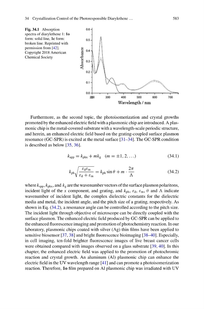
Fig. 34.1 Absorption
spectra of diarylethene 1: 1o
form: solid line, 1c form:
broken line. Reprinted with
permission from [42].
Copyright 2018 American
Chemical Society
Furthermore, as the second topic, the photoisomerization and crystal growths
promoted by the enhanced electric field with a plasmonic chip are introduced. A plasmonic chip is the metal-covered substrate with a wavelength-scale periodic structure,
and herein, an enhanced electric field based on the grating-coupled surface plasmon
resonance (GC-SPR) is excited at the metal surface [31–34]. The GC-SPR condition
is described as below [35, 36].
k spp = k phx + mk g (m = ±1, 2, . . .)
(34.1)
k ph
ε d ε m
ε d + ε m
= k ph sin θ + m ·
2π
(34.2)
where k spp , k phx , and k g are the wavenumber vectors of the surface plasmon polaritons,
incident light of the x component, and grating, and k ph , ε d , ε m , θ and indicate
wavenumber of incident light, the complex dielectric constants for the dielectric
media and metal, the incident angle, and the pitch size of a grating, respectively. As
shown in Eq. (34.2), a resonance angle can be controlled according to the pitch size.
The incident light through objective of microscope can be directly coupled with the
surface plasmon. The enhanced electric field produced by GC-SPR can be applied to
the enhanced fluorescence imaging and promotion of photochemistry reaction. In our
laboratory, plasmonic chips coated with silver (Ag) thin films have been applied to
sensitive biosensor [37, 38] and bright fluorescence bioimaging [38–40]. Especially,
in cell imaging, ten-fold brighter fluorescence images of live breast cancer cells
were obtained compared with images observed on a glass substrate [39, 40]. In this
chapter, the enhanced electric field was applied to the promotion of photochromic
reaction and crystal growth. An aluminum (Al) plasmonic chip can enhance the
electric field in the UV wavelength range [41] and can promote a photoisomerization
reaction. Therefore, 1o film prepared on Al plasmonic chip was irradiated with UV
583
Fig. 34.1 Absorption
spectra of diarylethene 1: 1o
form: solid line, 1c form:
broken line. Reprinted with
permission from [42].
Copyright 2018 American
Chemical Society
Furthermore, as the second topic, the photoisomerization and crystal growths
promoted by the enhanced electric field with a plasmonic chip are introduced. A plasmonic chip is the metal-covered substrate with a wavelength-scale periodic structure,
and herein, an enhanced electric field based on the grating-coupled surface plasmon
resonance (GC-SPR) is excited at the metal surface [31–34]. The GC-SPR condition
is described as below [35, 36].
k spp = k phx + mk g (m = ±1, 2, . . .)
(34.1)
k ph
ε d ε m
ε d + ε m
= k ph sin θ + m ·
2π
(34.2)
where k spp , k phx , and k g are the wavenumber vectors of the surface plasmon polaritons,
incident light of the x component, and grating, and k ph , ε d , ε m , θ and indicate
wavenumber of incident light, the complex dielectric constants for the dielectric
media and metal, the incident angle, and the pitch size of a grating, respectively. As
shown in Eq. (34.2), a resonance angle can be controlled according to the pitch size.
The incident light through objective of microscope can be directly coupled with the
surface plasmon. The enhanced electric field produced by GC-SPR can be applied to
the enhanced fluorescence imaging and promotion of photochemistry reaction. In our
laboratory, plasmonic chips coated with silver (Ag) thin films have been applied to
sensitive biosensor [37, 38] and bright fluorescence bioimaging [38–40]. Especially,
in cell imaging, ten-fold brighter fluorescence images of live breast cancer cells
were obtained compared with images observed on a glass substrate [39, 40]. In this
chapter, the enhanced electric field was applied to the promotion of photochromic
reaction and crystal growth. An aluminum (Al) plasmonic chip can enhance the
electric field in the UV wavelength range [41] and can promote a photoisomerization
reaction. Therefore, 1o film prepared on Al plasmonic chip was irradiated with UV