

10 Hot Carrier Transfer and Carrier Manipulation of Semiconductor …
189
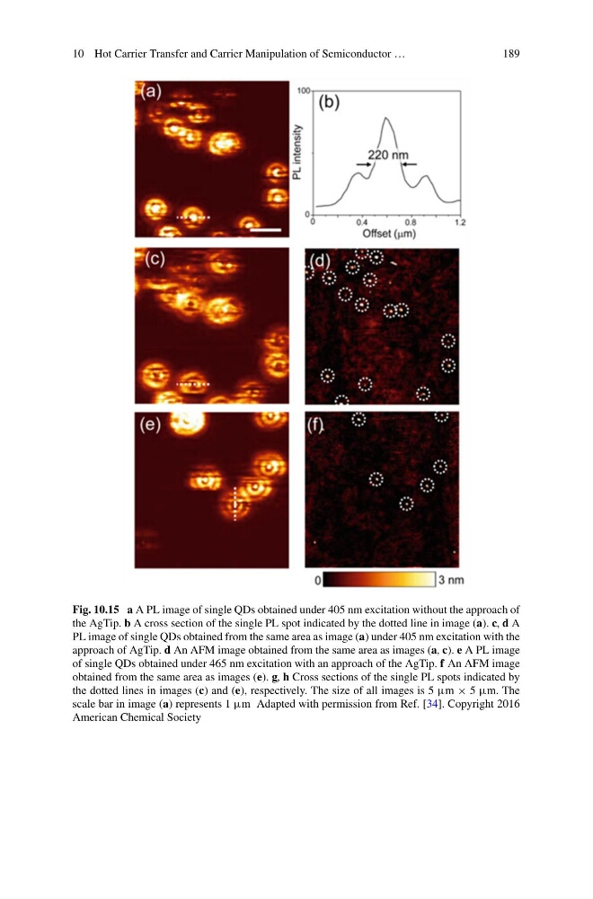
Fig. 10.15 a A PL image of single QDs obtained under 405 nm excitation without the approach of
the AgTip. b A cross section of the single PL spot indicated by the dotted line in image (a). c, d A
PL image of single QDs obtained from the same area as image (a) under 405 nm excitation with the
approach of AgTip. d An AFM image obtained from the same area as images (a, c). e A PL image
of single QDs obtained under 465 nm excitation with an approach of the AgTip. f An AFM image
obtained from the same area as images (e). g, h Cross sections of the single PL spots indicated by
the dotted lines in images (c) and (e), respectively. The size of all images is 5 μm × 5 μm. The
scale bar in image (a) represents 1 μm Adapted with permission from Ref. [34]. Copyright 2016
American Chemical Society
189
Fig. 10.15 a A PL image of single QDs obtained under 405 nm excitation without the approach of
the AgTip. b A cross section of the single PL spot indicated by the dotted line in image (a). c, d A
PL image of single QDs obtained from the same area as image (a) under 405 nm excitation with the
approach of AgTip. d An AFM image obtained from the same area as images (a, c). e A PL image
of single QDs obtained under 465 nm excitation with an approach of the AgTip. f An AFM image
obtained from the same area as images (e). g, h Cross sections of the single PL spots indicated by
the dotted lines in images (c) and (e), respectively. The size of all images is 5 μm × 5 μm. The
scale bar in image (a) represents 1 μm Adapted with permission from Ref. [34]. Copyright 2016
American Chemical Society