

Characterization Techniques in Nanotechnology …
45
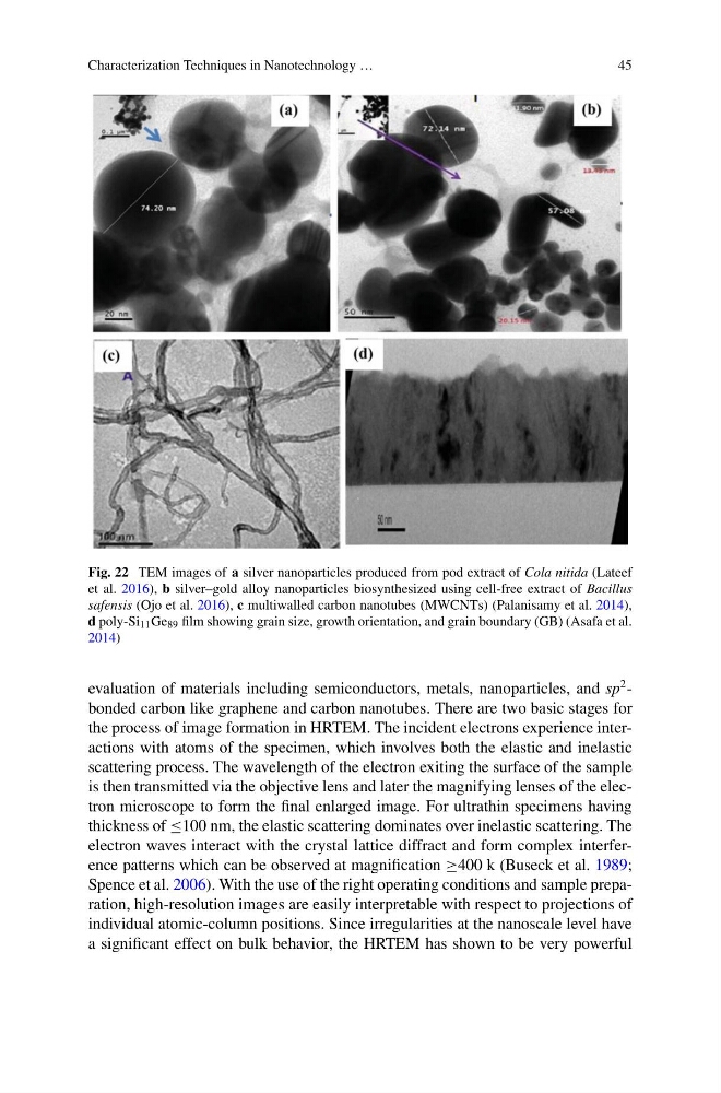
Fig. 22 TEM images of a silver nanoparticles produced from pod extract of Cola nitida (Lateef
et al. 2016), b silver–gold alloy nanoparticles biosynthesized using cell-free extract of Bacillus
safensis (Ojo et al. 2016), c multiwalled carbon nanotubes (MWCNTs) (Palanisamy et al. 2014),
d poly-Si 11 Ge 89 film showing grain size, growth orientation, and grain boundary (GB) (Asafa et al.
2014)
evaluation of materials including semiconductors, metals, nanoparticles, and sp
2 -
bonded carbon like graphene and carbon nanotubes. There are two basic stages for
the process of image formation in HRTEM. The incident electrons experience interactions with atoms of the specimen, which involves both the elastic and inelastic
scattering process. The wavelength of the electron exiting the surface of the sample
is then transmitted via the objective lens and later the magnifying lenses of the electron microscope to form the final enlarged image. For ultrathin specimens having
thickness of ≤100 nm, the elastic scattering dominates over inelastic scattering. The
electron waves interact with the crystal lattice diffract and form complex interference patterns which can be observed at magnification ≥400 k (Buseck et al. 1989;
Spence et al. 2006). With the use of the right operating conditions and sample preparation, high-resolution images are easily interpretable with respect to projections of
individual atomic-column positions. Since irregularities at the nanoscale level have
a significant effect on bulk behavior, the HRTEM has shown to be very powerful
45
Fig. 22 TEM images of a silver nanoparticles produced from pod extract of Cola nitida (Lateef
et al. 2016), b silver–gold alloy nanoparticles biosynthesized using cell-free extract of Bacillus
safensis (Ojo et al. 2016), c multiwalled carbon nanotubes (MWCNTs) (Palanisamy et al. 2014),
d poly-Si 11 Ge 89 film showing grain size, growth orientation, and grain boundary (GB) (Asafa et al.
2014)
evaluation of materials including semiconductors, metals, nanoparticles, and sp
2 -
bonded carbon like graphene and carbon nanotubes. There are two basic stages for
the process of image formation in HRTEM. The incident electrons experience interactions with atoms of the specimen, which involves both the elastic and inelastic
scattering process. The wavelength of the electron exiting the surface of the sample
is then transmitted via the objective lens and later the magnifying lenses of the electron microscope to form the final enlarged image. For ultrathin specimens having
thickness of ≤100 nm, the elastic scattering dominates over inelastic scattering. The
electron waves interact with the crystal lattice diffract and form complex interference patterns which can be observed at magnification ≥400 k (Buseck et al. 1989;
Spence et al. 2006). With the use of the right operating conditions and sample preparation, high-resolution images are easily interpretable with respect to projections of
individual atomic-column positions. Since irregularities at the nanoscale level have
a significant effect on bulk behavior, the HRTEM has shown to be very powerful