

Characterization Techniques in Nanotechnology …
39
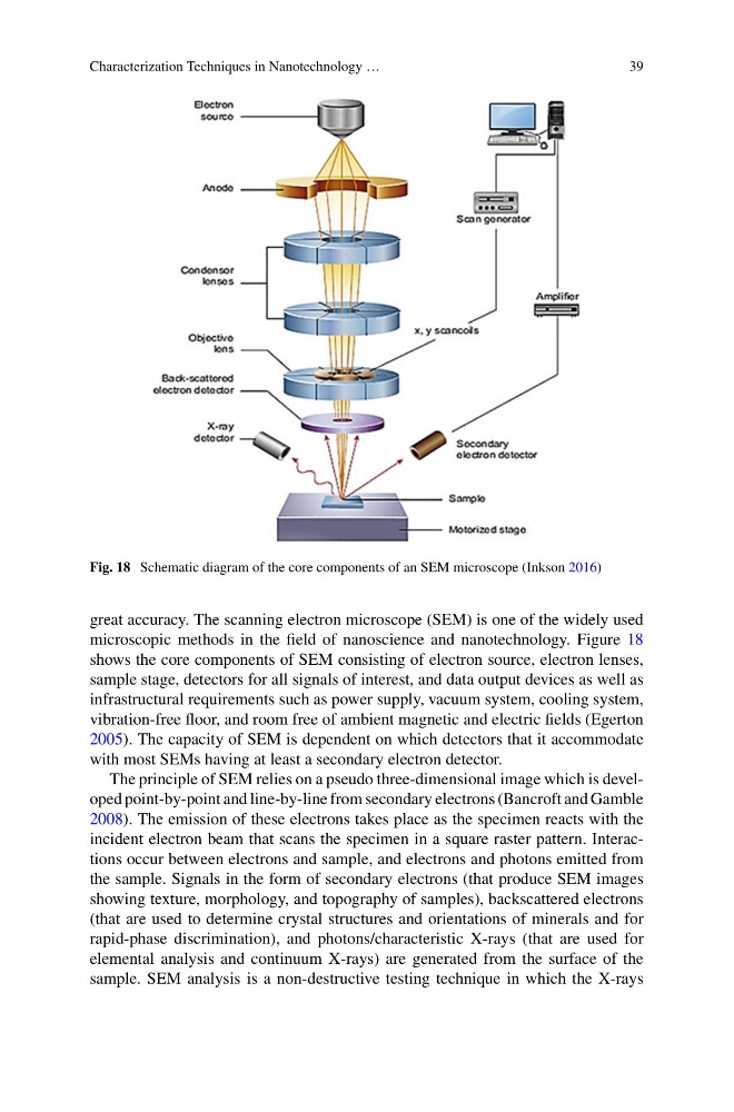
Fig. 18 Schematic diagram of the core components of an SEM microscope (Inkson 2016)
great accuracy. The scanning electron microscope (SEM) is one of the widely used
microscopic methods in the field of nanoscience and nanotechnology. Figure 18
shows the core components of SEM consisting of electron source, electron lenses,
sample stage, detectors for all signals of interest, and data output devices as well as
infrastructural requirements such as power supply, vacuum system, cooling system,
vibration-free floor, and room free of ambient magnetic and electric fields (Egerton
2005). The capacity of SEM is dependent on which detectors that it accommodate
with most SEMs having at least a secondary electron detector.
The principle of SEM relies on a pseudo three-dimensional image which is developed point-by-point and line-by-line from secondary electrons (Bancroft and Gamble
2008). The emission of these electrons takes place as the specimen reacts with the
incident electron beam that scans the specimen in a square raster pattern. Interactions occur between electrons and sample, and electrons and photons emitted from
the sample. Signals in the form of secondary electrons (that produce SEM images
showing texture, morphology, and topography of samples), backscattered electrons
(that are used to determine crystal structures and orientations of minerals and for
rapid-phase discrimination), and photons/characteristic X-rays (that are used for
elemental analysis and continuum X-rays) are generated from the surface of the
sample. SEM analysis is a non-destructive testing technique in which the X-rays
39
Fig. 18 Schematic diagram of the core components of an SEM microscope (Inkson 2016)
great accuracy. The scanning electron microscope (SEM) is one of the widely used
microscopic methods in the field of nanoscience and nanotechnology. Figure 18
shows the core components of SEM consisting of electron source, electron lenses,
sample stage, detectors for all signals of interest, and data output devices as well as
infrastructural requirements such as power supply, vacuum system, cooling system,
vibration-free floor, and room free of ambient magnetic and electric fields (Egerton
2005). The capacity of SEM is dependent on which detectors that it accommodate
with most SEMs having at least a secondary electron detector.
The principle of SEM relies on a pseudo three-dimensional image which is developed point-by-point and line-by-line from secondary electrons (Bancroft and Gamble
2008). The emission of these electrons takes place as the specimen reacts with the
incident electron beam that scans the specimen in a square raster pattern. Interactions occur between electrons and sample, and electrons and photons emitted from
the sample. Signals in the form of secondary electrons (that produce SEM images
showing texture, morphology, and topography of samples), backscattered electrons
(that are used to determine crystal structures and orientations of minerals and for
rapid-phase discrimination), and photons/characteristic X-rays (that are used for
elemental analysis and continuum X-rays) are generated from the surface of the
sample. SEM analysis is a non-destructive testing technique in which the X-rays