

38
T. B. Asafa et al.
the ZnO and Ag–ZnO samples which is ascribed to the presence of carbon on the
surface of the films (Patil et al. 2015). The difference between the peaks at 372.9
(Ag 3d5/2) and 367 eV (3d3/2) implies the presence of metallic Ag and Ag–Zn–O
ternary compounds, respectively, as shown in Fig. 17d.
2 Microscopy
Microscopy plays an important role in the field of nanotechnology as it is employed
to generate images for the morphological studies of nanomaterials including surface
roughness, topology, exact particles size, distribution, and thickness. Microscopy
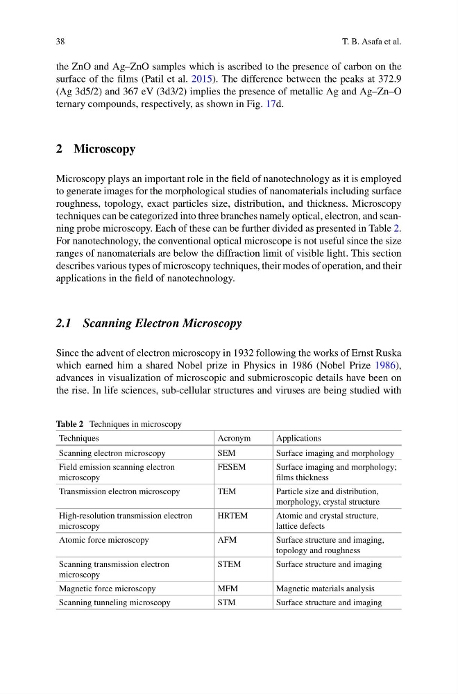
techniques can be categorized into three branches namely optical, electron, and scanning probe microscopy. Each of these can be further divided as presented in Table 2.
For nanotechnology, the conventional optical microscope is not useful since the size
ranges of nanomaterials are below the diffraction limit of visible light. This section
describes various types of microscopy techniques, their modes of operation, and their
applications in the field of nanotechnology.
2.1 Scanning Electron Microscopy
Since the advent of electron microscopy in 1932 following the works of Ernst Ruska
which earned him a shared Nobel prize in Physics in 1986 (Nobel Prize 1986),
advances in visualization of microscopic and submicroscopic details have been on
the rise. In life sciences, sub-cellular structures and viruses are being studied with
Table 2 Techniques in microscopy
Techniques
Acronym
Applications
Scanning electron microscopy
SEM
Surface imaging and morphology
Field emission scanning electron
microscopy
FESEM
Surface imaging and morphology;
films thickness
Transmission electron microscopy
TEM
Particle size and distribution,
morphology, crystal structure
High-resolution transmission electron
microscopy
HRTEM
Atomic and crystal structure,
lattice defects
Atomic force microscopy
AFM
Surface structure and imaging,
topology and roughness
Scanning transmission electron
microscopy
STEM
Surface structure and imaging
Magnetic force microscopy
MFM
Magnetic materials analysis
Scanning tunneling microscopy
STM
Surface structure and imaging
T. B. Asafa et al.
the ZnO and Ag–ZnO samples which is ascribed to the presence of carbon on the
surface of the films (Patil et al. 2015). The difference between the peaks at 372.9
(Ag 3d5/2) and 367 eV (3d3/2) implies the presence of metallic Ag and Ag–Zn–O
ternary compounds, respectively, as shown in Fig. 17d.
2 Microscopy
Microscopy plays an important role in the field of nanotechnology as it is employed
to generate images for the morphological studies of nanomaterials including surface
roughness, topology, exact particles size, distribution, and thickness. Microscopy
techniques can be categorized into three branches namely optical, electron, and scanning probe microscopy. Each of these can be further divided as presented in Table 2.
For nanotechnology, the conventional optical microscope is not useful since the size
ranges of nanomaterials are below the diffraction limit of visible light. This section
describes various types of microscopy techniques, their modes of operation, and their
applications in the field of nanotechnology.
2.1 Scanning Electron Microscopy
Since the advent of electron microscopy in 1932 following the works of Ernst Ruska
which earned him a shared Nobel prize in Physics in 1986 (Nobel Prize 1986),
advances in visualization of microscopic and submicroscopic details have been on
the rise. In life sciences, sub-cellular structures and viruses are being studied with
Table 2 Techniques in microscopy
Techniques
Acronym
Applications
Scanning electron microscopy
SEM
Surface imaging and morphology
Field emission scanning electron
microscopy
FESEM
Surface imaging and morphology;
films thickness
Transmission electron microscopy
TEM
Particle size and distribution,
morphology, crystal structure
High-resolution transmission electron
microscopy
HRTEM
Atomic and crystal structure,
lattice defects
Atomic force microscopy
AFM
Surface structure and imaging,
topology and roughness
Scanning transmission electron
microscopy
STEM
Surface structure and imaging
Magnetic force microscopy
MFM
Magnetic materials analysis
Scanning tunneling microscopy
STM
Surface structure and imaging