

142
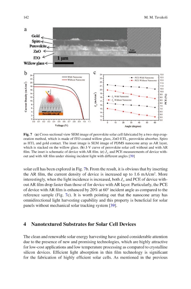
solar cell has been explored in Fig. 7b. From the result, it is obvious that by inserting
the AR film, the current density of device is increased up to 1.6 mA/cm
2
. More
interestingly, when the light incidence is increased, both J sc and PCE of device without AR film drop faster than those of for device with AR layer. Particularly, the PCE
of device with AR film is enhanced by 20% at 60° incident angle as compared to the
reference sample (Fig. 7c). It is worth pointing out that the nanocone array has
omnidirectional light harvesting capability and this property is beneficial for solar
panels without mechanical solar tracking system [39].
4 Nanotextured Substrates for Solar Cell Devices
The clean and renewable solar energy harvesting have gained considerable attention
due to the presence of new and promising technologies, which are highly attractive
for low-cost applications and low temperature processing as compared to crystalline
silicon devices. Efficient light absorption in thin film technology is significant
for the fabrication of highly efficient solar cells. As mentioned in the previous
Fig. 7 (a) Cross-sectional view SEM image of perovskite solar cell fabricated by a two-step evaporation method, which is made of ITO coated willow glass, ZnO ETL, perovskite absorber, Spiro
as HTL and gold contact. The inset image is SEM image of PDMS nanocone array as AR layer,
which is stacked on the willow glass. (b) J-V curve of perovskite solar cell without and with AR
film. The inset is schematic of device with AR film. (c) J sc and PCE measurements of device without and with AR film under shining incident light with different angles [39]
M. M. Tavakoli
solar cell has been explored in Fig. 7b. From the result, it is obvious that by inserting
the AR film, the current density of device is increased up to 1.6 mA/cm
2
. More
interestingly, when the light incidence is increased, both J sc and PCE of device without AR film drop faster than those of for device with AR layer. Particularly, the PCE
of device with AR film is enhanced by 20% at 60° incident angle as compared to the
reference sample (Fig. 7c). It is worth pointing out that the nanocone array has
omnidirectional light harvesting capability and this property is beneficial for solar
panels without mechanical solar tracking system [39].
4 Nanotextured Substrates for Solar Cell Devices
The clean and renewable solar energy harvesting have gained considerable attention
due to the presence of new and promising technologies, which are highly attractive
for low-cost applications and low temperature processing as compared to crystalline
silicon devices. Efficient light absorption in thin film technology is significant
for the fabrication of highly efficient solar cells. As mentioned in the previous
Fig. 7 (a) Cross-sectional view SEM image of perovskite solar cell fabricated by a two-step evaporation method, which is made of ITO coated willow glass, ZnO ETL, perovskite absorber, Spiro
as HTL and gold contact. The inset image is SEM image of PDMS nanocone array as AR layer,
which is stacked on the willow glass. (b) J-V curve of perovskite solar cell without and with AR
film. The inset is schematic of device with AR film. (c) J sc and PCE measurements of device without and with AR film under shining incident light with different angles [39]
M. M. Tavakoli