

135
In fact, for an ideal Lambertian scatterer with an isotropic radiance, the value of
radiance (L) is equal to 1/π. However for an arbitrary scatterer, the value of L is
depended on the refractive indices of both medias and the surface morphology (z(x,
y)) of the interface. For example, in a silicon solar cell, consisted of a glass substrate
with refractive index of ~1.5, a transparent electrode (n ~ 2) and the silicon absorber
(n ~ 4), by texturing the electrode/silicon interface, light scattering can be achieved.
Here, the scattering of light from the electrode to air is so close to Lambertian and
more importantly the fraction of the scattered light shows an angular dependence
with respect to the Lambertian scatterer. In order to consider scattering into the silicon layer, it is proved that the height (Z) has to be scaled by1/2 and the lateral
dimensions should be scaled by 1/4. Consequently, for the case of Lambertian scatterer to silicon, it is required to do a reduction in feature size by a factor of 4 and an
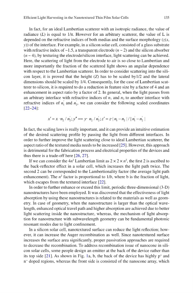
enhancement in aspect ratio by a factor of 2. In general, when the light passes from
an arbitrary interface with refractive indices of n 1 and n 2 to another interface with
refractive indices of n 1
′ and n 2
′ , we can consider the following scaled coordinates
[22–24]:
′
′ ′
′
=
= =
=
−
−
′
′
′
′
x x n n y
y n n z z n n
n n
· / ;
· / ;
·|
| / |
|
2
2
2
2
1
2
1
2
In fact, the scaling laws is really important, and it can provide an intuitive estimation
of the desired scattering profile by passing the light from different interfaces. In
order to further improve the light scattering close to ideal Lambertian scatterer, the
aspect ratio of the textured media needs to be increased [25]. However, this approach
is detrimental for the fabrication process and electrical properties of the devices and
thus there is a trade-off here [26, 27].
If we can consider the 4n
2
Lambertian limit as 2 × 2 × n
2
, the first 2 is ascribed to
the back-reflector effect in a solar cell, which increases the light path twice. The
second 2 can be corresponded to the Lambertionality factor (the average light path
enhancement). The n
2
factor is proportional to 1/b, where b is the fraction of light,
which escapes from the textured interface [22].
In order to further enhance or exceed this limit, periodic three-dimensional (3-D)
nanostructures have been employed. It was discovered that the effectiveness of light
absorption by using these nanostructures is related to the materials as well as geometry. In case of geometry, when the nanostructure is larger than the optical wavelength, enhanced optical travel path and higher absorption are achieved due to better
light scattering inside the nanostructure, whereas, the mechanism of light absorption for nanostructure with subwavelength geometry can be fundamental photonic
resonant modes due to light confinement.
In a silicon solar cell, nanotextured surface can reduce the light reflection; however, it can increase the Auger recombination as well. Since nanotextured surface
increases the surface area significantly, proper passivation approaches are required
to decrease the recombination. To address recombination issue of nanocone in silicon solar cells, some people design an emitter at the back of the device rather than
its top side [21]. As shown in Fig. 1a, b, the back of the device has highly p
+
and
n
−
doped regions, whereas the front side is consisted of the nanocone array, which
Efficient Light Harvesting in the Nanotextured Thin Film Solar Cells
In fact, for an ideal Lambertian scatterer with an isotropic radiance, the value of
radiance (L) is equal to 1/π. However for an arbitrary scatterer, the value of L is
depended on the refractive indices of both medias and the surface morphology (z(x,
y)) of the interface. For example, in a silicon solar cell, consisted of a glass substrate
with refractive index of ~1.5, a transparent electrode (n ~ 2) and the silicon absorber
(n ~ 4), by texturing the electrode/silicon interface, light scattering can be achieved.
Here, the scattering of light from the electrode to air is so close to Lambertian and
more importantly the fraction of the scattered light shows an angular dependence
with respect to the Lambertian scatterer. In order to consider scattering into the silicon layer, it is proved that the height (Z) has to be scaled by1/2 and the lateral
dimensions should be scaled by 1/4. Consequently, for the case of Lambertian scatterer to silicon, it is required to do a reduction in feature size by a factor of 4 and an
enhancement in aspect ratio by a factor of 2. In general, when the light passes from
an arbitrary interface with refractive indices of n 1 and n 2 to another interface with
refractive indices of n 1
′ and n 2
′ , we can consider the following scaled coordinates
[22–24]:
′
′ ′
′
=
= =
=
−
−
′
′
′
′
x x n n y
y n n z z n n
n n
· / ;
· / ;
·|
| / |
|
2
2
2
2
1
2
1
2
In fact, the scaling laws is really important, and it can provide an intuitive estimation
of the desired scattering profile by passing the light from different interfaces. In
order to further improve the light scattering close to ideal Lambertian scatterer, the
aspect ratio of the textured media needs to be increased [25]. However, this approach
is detrimental for the fabrication process and electrical properties of the devices and
thus there is a trade-off here [26, 27].
If we can consider the 4n
2
Lambertian limit as 2 × 2 × n
2
, the first 2 is ascribed to
the back-reflector effect in a solar cell, which increases the light path twice. The
second 2 can be corresponded to the Lambertionality factor (the average light path
enhancement). The n
2
factor is proportional to 1/b, where b is the fraction of light,
which escapes from the textured interface [22].
In order to further enhance or exceed this limit, periodic three-dimensional (3-D)
nanostructures have been employed. It was discovered that the effectiveness of light
absorption by using these nanostructures is related to the materials as well as geometry. In case of geometry, when the nanostructure is larger than the optical wavelength, enhanced optical travel path and higher absorption are achieved due to better
light scattering inside the nanostructure, whereas, the mechanism of light absorption for nanostructure with subwavelength geometry can be fundamental photonic
resonant modes due to light confinement.
In a silicon solar cell, nanotextured surface can reduce the light reflection; however, it can increase the Auger recombination as well. Since nanotextured surface
increases the surface area significantly, proper passivation approaches are required
to decrease the recombination. To address recombination issue of nanocone in silicon solar cells, some people design an emitter at the back of the device rather than
its top side [21]. As shown in Fig. 1a, b, the back of the device has highly p
+
and
n
−
doped regions, whereas the front side is consisted of the nanocone array, which
Efficient Light Harvesting in the Nanotextured Thin Film Solar Cells