

134
that the optical absorption and J sc are increased monotonically with NSP height. The
inset image in Fig. 2f illustrates the absorption profile of the device based on NSP
with 1.2 μm height, indicating that the most of absorption occurred in the active a-Si
active layer. Moreover, it can be concluded that by increasing the pitch size for the
same height, the optical absorption is decreased due to lower light scattering with
large NSP to NSP distance in large pitch [16].
3 Anti-reflection Nanostructures for Solar Cell Devices
Enhancing the Light absorption of Anti-reflection (AR) nanostructures the active
layer in the optoelectronic devices is necessary step to boost the device performance. To satisfy this purpose, there are two general strategies, first, increase the
optical absorption and decrease the reflectance by using the anti-reflection (AR)
layer and second, increase the absorption through the surface of nanostructure.
Among AR methods, anti-reflection coating is a common way, which is typically
utilized for enhancement of light absorption. However, this technique needs several
coating layers to achieve a broad-band absorption, results in higher production cost.
For the absorption enhancement methods, random nanotextured surface and back
metal reflector are usually employed. In fact, the absorption can increase up to the
Lambertian limit of 4N
2
, where N is the refractive index [20, 21]. Basically, when
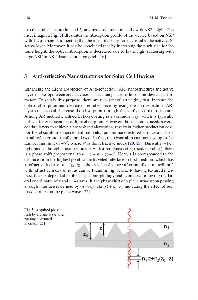
light passes through a textured media with a roughness of z 0 (peak to valley), there
is a phase shift proportional to n 1 · z + n 2 · (z 0 −z). Here, z is corresponded to the
distance from the highest point to the traveled interface in first medium, which has
a refractive index of n 1 · (z 0 −z) is the traveled distance after interface in medium 2
with refractive index of n 2 , as can be found in Fig. 3. Due to having textured interface, the z is depended on the surface morphology and geometry, following the lateral coordinates of x and y. As a result, the phase shift of a plane wave upon passing
a rough interface is defined by (n 1 −n 2 ) · z(x, y) + n 2 · z 0 , indicating the effect of textured surface on the plane wave [22].
Fig. 3 Acquired phase
shift by a plane wave after
passing a textured
interface [22]
M. M. Tavakoli
that the optical absorption and J sc are increased monotonically with NSP height. The
inset image in Fig. 2f illustrates the absorption profile of the device based on NSP
with 1.2 μm height, indicating that the most of absorption occurred in the active a-Si
active layer. Moreover, it can be concluded that by increasing the pitch size for the
same height, the optical absorption is decreased due to lower light scattering with
large NSP to NSP distance in large pitch [16].
3 Anti-reflection Nanostructures for Solar Cell Devices
Enhancing the Light absorption of Anti-reflection (AR) nanostructures the active
layer in the optoelectronic devices is necessary step to boost the device performance. To satisfy this purpose, there are two general strategies, first, increase the
optical absorption and decrease the reflectance by using the anti-reflection (AR)
layer and second, increase the absorption through the surface of nanostructure.
Among AR methods, anti-reflection coating is a common way, which is typically
utilized for enhancement of light absorption. However, this technique needs several
coating layers to achieve a broad-band absorption, results in higher production cost.
For the absorption enhancement methods, random nanotextured surface and back
metal reflector are usually employed. In fact, the absorption can increase up to the
Lambertian limit of 4N
2
, where N is the refractive index [20, 21]. Basically, when
light passes through a textured media with a roughness of z 0 (peak to valley), there
is a phase shift proportional to n 1 · z + n 2 · (z 0 −z). Here, z is corresponded to the
distance from the highest point to the traveled interface in first medium, which has
a refractive index of n 1 · (z 0 −z) is the traveled distance after interface in medium 2
with refractive index of n 2 , as can be found in Fig. 3. Due to having textured interface, the z is depended on the surface morphology and geometry, following the lateral coordinates of x and y. As a result, the phase shift of a plane wave upon passing
a rough interface is defined by (n 1 −n 2 ) · z(x, y) + n 2 · z 0 , indicating the effect of textured surface on the plane wave [22].
Fig. 3 Acquired phase
shift by a plane wave after
passing a textured
interface [22]
M. M. Tavakoli