

18 Interfacial Materials for Organic Solar Cells
375
In addition to the synthesis of novel active layer materials and updated device fabrication conditions, the design and implementation of interfacial materials is also very
crucial in the device performance improvement. An ideal interfacial design is most
important for efficient charge transport as they not only establish good Ohmic contact
but also regulate other device parameters like film morphology, control energy level
alignment, alter work functions (WF) of both anode and cathode, minimize resistance with high charge selectivity, reduce charge recombination rate, enhance charge
extraction and improve device stability (Ma et al. 2010; Chen et al. 2010). The WF
is defined as the energy difference between Fermi energy and vacuum level which is
the minimum amount of energy necessary to withdraw an electron from the metal. In
order to match the energy levels for efficient charge transport and collections various
cathode and anode interfacial layers have been introduced between the active layer
and electrodes. To date, several reports have revealed the underlying mechanisms for
the tuning of WF by interfacial materials at the active layer/electrode interfaces (van
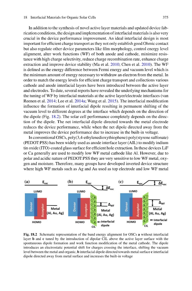
Reenen et al. 2014; Lee et al. 2014a; Wang et al. 2015). The interfacial modification
influence the formation of interfacial dipole resulting in permanent shifting of the
vacuum level to different degrees at the interface which depends on the direction of
the dipole (Fig. 18.2). The solar cell performance completely depends on the direction of the dipole. The net interfacial dipole directed towards the metal electrode
reduces the device performance, while when the net dipole directed away from the
metal improves the device performance due to increase in the built-in voltage.
In conventional OSCs, poly(3,4-ethylenedioxythiophene):poly(styrene sulfonate)
(PEDOT:PSS) has been widely used as anode interface layer (AIL) to modify indium
tin oxide (ITO)-coated glass surface for efficient hole extraction. In these devices LiF
or Ca generally are used to modify low WF metal cathode like Al. However, due to
polar and acidic nature of PEDOT:PSS they are very sensitive to low WF metal, oxygen and moisture. Therefore, many groups have developed inverted device structure
where high WF metals such as Ag and Au used as top electrode and low WF metal
Fig. 18.2 Schematic representation of the band energy alignment for OSCs a without interfacial
layer b and c tuned by the introduction of dipolar CIL above the active layer surface with the
spontaneous dipole formation and work function modification of the metal cathode. The dipole
introduces an electrostatic potential shift for charges crossing the interface, shifting the vacuum
level between the metal and organic, b interfacial dipole directed towards metal surface c interfacial
dipole directed away from metal surface and increases the built-in voltage
375
In addition to the synthesis of novel active layer materials and updated device fabrication conditions, the design and implementation of interfacial materials is also very
crucial in the device performance improvement. An ideal interfacial design is most
important for efficient charge transport as they not only establish good Ohmic contact
but also regulate other device parameters like film morphology, control energy level
alignment, alter work functions (WF) of both anode and cathode, minimize resistance with high charge selectivity, reduce charge recombination rate, enhance charge
extraction and improve device stability (Ma et al. 2010; Chen et al. 2010). The WF
is defined as the energy difference between Fermi energy and vacuum level which is
the minimum amount of energy necessary to withdraw an electron from the metal. In
order to match the energy levels for efficient charge transport and collections various
cathode and anode interfacial layers have been introduced between the active layer
and electrodes. To date, several reports have revealed the underlying mechanisms for
the tuning of WF by interfacial materials at the active layer/electrode interfaces (van
Reenen et al. 2014; Lee et al. 2014a; Wang et al. 2015). The interfacial modification
influence the formation of interfacial dipole resulting in permanent shifting of the
vacuum level to different degrees at the interface which depends on the direction of
the dipole (Fig. 18.2). The solar cell performance completely depends on the direction of the dipole. The net interfacial dipole directed towards the metal electrode
reduces the device performance, while when the net dipole directed away from the
metal improves the device performance due to increase in the built-in voltage.
In conventional OSCs, poly(3,4-ethylenedioxythiophene):poly(styrene sulfonate)
(PEDOT:PSS) has been widely used as anode interface layer (AIL) to modify indium
tin oxide (ITO)-coated glass surface for efficient hole extraction. In these devices LiF
or Ca generally are used to modify low WF metal cathode like Al. However, due to
polar and acidic nature of PEDOT:PSS they are very sensitive to low WF metal, oxygen and moisture. Therefore, many groups have developed inverted device structure
where high WF metals such as Ag and Au used as top electrode and low WF metal
Fig. 18.2 Schematic representation of the band energy alignment for OSCs a without interfacial
layer b and c tuned by the introduction of dipolar CIL above the active layer surface with the
spontaneous dipole formation and work function modification of the metal cathode. The dipole
introduces an electrostatic potential shift for charges crossing the interface, shifting the vacuum
level between the metal and organic, b interfacial dipole directed towards metal surface c interfacial
dipole directed away from metal surface and increases the built-in voltage