

46
A. Shah
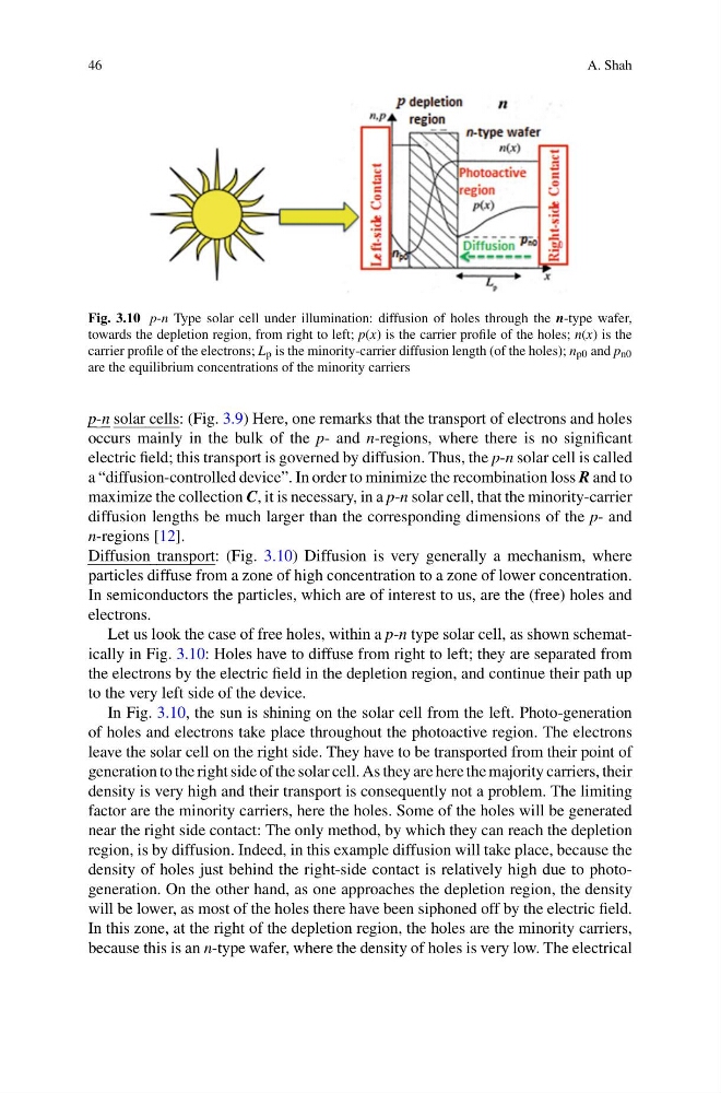
Fig. 3.10 p-n Type solar cell under illumination: diffusion of holes through the n-type wafer,
towards the depletion region, from right to left; p(x) is the carrier profile of the holes; n(x) is the
carrier profile of the electrons; L p is the minority-carrier diffusion length (of the holes); n p0 and p n0
are the equilibrium concentrations of the minority carriers
p-n solar cells: (Fig. 3.9) Here, one remarks that the transport of electrons and holes
occurs mainly in the bulk of the p- and n-regions, where there is no significant
electric field; this transport is governed by diffusion. Thus, the p-n solar cell is called
a “diffusion-controlled device”. In order to minimize the recombination loss R and to
maximize the collection C, it is necessary, in a p-n solar cell, that the minority-carrier
diffusion lengths be much larger than the corresponding dimensions of the p- and
n-regions [12].
Diffusion transport: (Fig. 3.10) Diffusion is very generally a mechanism, where
particles diffuse from a zone of high concentration to a zone of lower concentration.
In semiconductors the particles, which are of interest to us, are the (free) holes and
electrons.
Let us look the case of free holes, within a p-n type solar cell, as shown schematically in Fig. 3.10: Holes have to diffuse from right to left; they are separated from
the electrons by the electric field in the depletion region, and continue their path up
to the very left side of the device.
In Fig. 3.10, the sun is shining on the solar cell from the left. Photo-generation
of holes and electrons take place throughout the photoactive region. The electrons
leave the solar cell on the right side. They have to be transported from their point of
generation to the right side of the solar cell. As they are here the majority carriers, their
density is very high and their transport is consequently not a problem. The limiting
factor are the minority carriers, here the holes. Some of the holes will be generated
near the right side contact: The only method, by which they can reach the depletion
region, is by diffusion. Indeed, in this example diffusion will take place, because the
density of holes just behind the right-side contact is relatively high due to photogeneration. On the other hand, as one approaches the depletion region, the density
will be lower, as most of the holes there have been siphoned off by the electric field.
In this zone, at the right of the depletion region, the holes are the minority carriers,
because this is an n-type wafer, where the density of holes is very low. The electrical
A. Shah
Fig. 3.10 p-n Type solar cell under illumination: diffusion of holes through the n-type wafer,
towards the depletion region, from right to left; p(x) is the carrier profile of the holes; n(x) is the
carrier profile of the electrons; L p is the minority-carrier diffusion length (of the holes); n p0 and p n0
are the equilibrium concentrations of the minority carriers
p-n solar cells: (Fig. 3.9) Here, one remarks that the transport of electrons and holes
occurs mainly in the bulk of the p- and n-regions, where there is no significant
electric field; this transport is governed by diffusion. Thus, the p-n solar cell is called
a “diffusion-controlled device”. In order to minimize the recombination loss R and to
maximize the collection C, it is necessary, in a p-n solar cell, that the minority-carrier
diffusion lengths be much larger than the corresponding dimensions of the p- and
n-regions [12].
Diffusion transport: (Fig. 3.10) Diffusion is very generally a mechanism, where
particles diffuse from a zone of high concentration to a zone of lower concentration.
In semiconductors the particles, which are of interest to us, are the (free) holes and
electrons.
Let us look the case of free holes, within a p-n type solar cell, as shown schematically in Fig. 3.10: Holes have to diffuse from right to left; they are separated from
the electrons by the electric field in the depletion region, and continue their path up
to the very left side of the device.
In Fig. 3.10, the sun is shining on the solar cell from the left. Photo-generation
of holes and electrons take place throughout the photoactive region. The electrons
leave the solar cell on the right side. They have to be transported from their point of
generation to the right side of the solar cell. As they are here the majority carriers, their
density is very high and their transport is consequently not a problem. The limiting
factor are the minority carriers, here the holes. Some of the holes will be generated
near the right side contact: The only method, by which they can reach the depletion
region, is by diffusion. Indeed, in this example diffusion will take place, because the
density of holes just behind the right-side contact is relatively high due to photogeneration. On the other hand, as one approaches the depletion region, the density
will be lower, as most of the holes there have been siphoned off by the electric field.
In this zone, at the right of the depletion region, the holes are the minority carriers,
because this is an n-type wafer, where the density of holes is very low. The electrical