

1 Introduction
9
• Reduced energy in the preparation of pure polysilicon: the most energy-intensive
step is crystallization of polysilicon from a purified gas containing silicon. This
is done in what is known as a “Siemens reactor”. Today’s reactors use multiple
filaments or tubular filaments, to speed up polysilicon deposition, and highlyreflective coated jars to keep the wall colder. They can produce up to 10 tons of
polysilicon per run, ensuring energy usage in the range of 40–50 kWh per kg of
silicon [7], against 130–250 kWh per kg a decade ago.
• Reduction in the amount of silicon per wafer thanks to advanced multi-wire sawing: Between 2016 and 2019, the entire industry switched from SiC-slurry based
multi-wire sawing to diamond wire sawing. In the latter process, steel wires incorporating small diamonds are used to cut the ingot into wafers. The typical kerf
loss (material losses) between two wafers of 150–200 microns has been quickly
reduced down to 60 microns, allowing an increase of 30–40% in the number of
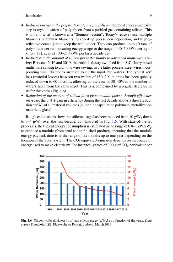
wafers sawn from the same ingot. This is accompanied by a regular decrease in
wafer thickness (Fig. 1.6).
• Reduction of the amount of silicon for a given module power, through efficiency
increase: the 3–4% gain in efficiency during the last decade allows a direct reduction per W p of all material volumes (silicon, encapsulation polymers, metallization
materials, glass).
Rough calculations show that silicon usage has been reduced from 10 g/W p down
to 3–4 g/W p over the last decade, as illustrated in Fig. 1.6. With state-of-the-art
processes, the typical energy consumption is estimated in the range of 0.8–1 kWh/W p
to produce a module (from sand to the finished product), meaning that the module
energy payback time is in the range of six months up to one year depending on the
location of the Solar system. The CO 2 equivalent emission depends on the source of
energy used to make electricity. For instance, values of 300 g of CO 2 equivalent per
Fig. 1.6 Silicon wafer thickness [µm] and silicon usage [g/W p ] as a function of the years. Data
source Fraunhofer ISE: Photovoltaics Report, updated: March 2019
9
• Reduced energy in the preparation of pure polysilicon: the most energy-intensive
step is crystallization of polysilicon from a purified gas containing silicon. This
is done in what is known as a “Siemens reactor”. Today’s reactors use multiple
filaments or tubular filaments, to speed up polysilicon deposition, and highlyreflective coated jars to keep the wall colder. They can produce up to 10 tons of
polysilicon per run, ensuring energy usage in the range of 40–50 kWh per kg of
silicon [7], against 130–250 kWh per kg a decade ago.
• Reduction in the amount of silicon per wafer thanks to advanced multi-wire sawing: Between 2016 and 2019, the entire industry switched from SiC-slurry based
multi-wire sawing to diamond wire sawing. In the latter process, steel wires incorporating small diamonds are used to cut the ingot into wafers. The typical kerf
loss (material losses) between two wafers of 150–200 microns has been quickly
reduced down to 60 microns, allowing an increase of 30–40% in the number of
wafers sawn from the same ingot. This is accompanied by a regular decrease in
wafer thickness (Fig. 1.6).
• Reduction of the amount of silicon for a given module power, through efficiency
increase: the 3–4% gain in efficiency during the last decade allows a direct reduction per W p of all material volumes (silicon, encapsulation polymers, metallization
materials, glass).
Rough calculations show that silicon usage has been reduced from 10 g/W p down
to 3–4 g/W p over the last decade, as illustrated in Fig. 1.6. With state-of-the-art
processes, the typical energy consumption is estimated in the range of 0.8–1 kWh/W p
to produce a module (from sand to the finished product), meaning that the module
energy payback time is in the range of six months up to one year depending on the
location of the Solar system. The CO 2 equivalent emission depends on the source of
energy used to make electricity. For instance, values of 300 g of CO 2 equivalent per
Fig. 1.6 Silicon wafer thickness [µm] and silicon usage [g/W p ] as a function of the years. Data
source Fraunhofer ISE: Photovoltaics Report, updated: March 2019