

9 Solar Module Technology
221
the cell busbar. In some cases, as for HJT cells that require low-temperature processes
to avoid damaging the passivating layers, electrically conductive adhesives (ECA)
are used in the place of soldering. As of today, most solar cells have four or five
busbars (4BB-5BB). An increased number of busbars or even multi-wire concepts
with no busbars can be expected in future PV modules, as this will lead to reduced
silver consumption; it should also lead to a reduction in the vulnerability of module
performance to cell cracks and breakage (see Sect. 9.3). IBC (Interdigitated Back
Contact) cells as well, where both positive and negative contacts are at the rear side
of the cell, do not need busbars. To connect neighbouring cells, the ribbons are placed
on the rear side of the cells.
Similarly, thin film modules can be manufactured by contacting adjacent solar
cells with ribbons. However, this is usually done in a similar way by using the
so-called monolithic interconnection of cells. This method constitutes one of the
advantages of thin film technologies as compared to wafer-based ones. In this process, semiconductor and metal layers are deposited over the full surface of a substrate.
The solar cells are then separated by means of laser or mechanical scribes, which are
performed sequentially. The front side of a solar cell is generally connected to the rear
side of the adjacent cell by means of the transparent conductive oxide (TCO) layer,
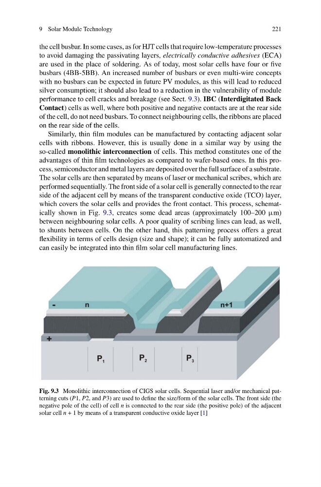
which covers the solar cells and provides the front contact. This process, schematically shown in Fig. 9.3, creates some dead areas (approximately 100–200 μm)
between neighbouring solar cells. A poor quality of scribing lines can lead, as well,
to shunts between cells. On the other hand, this patterning process offers a great
flexibility in terms of cells design (size and shape); it can be fully automatized and
can easily be integrated into thin film solar cell manufacturing lines.
Fig. 9.3 Monolithic interconnection of CIGS solar cells. Sequential laser and/or mechanical patterning cuts (P1, P2, and P3) are used to define the size/form of the solar cells. The front side (the
negative pole of the cell) of cell n is connected to the rear side (the positive pole) of the adjacent
solar cell n + 1 by means of a transparent conductive oxide layer [1]
221
the cell busbar. In some cases, as for HJT cells that require low-temperature processes
to avoid damaging the passivating layers, electrically conductive adhesives (ECA)
are used in the place of soldering. As of today, most solar cells have four or five
busbars (4BB-5BB). An increased number of busbars or even multi-wire concepts
with no busbars can be expected in future PV modules, as this will lead to reduced
silver consumption; it should also lead to a reduction in the vulnerability of module
performance to cell cracks and breakage (see Sect. 9.3). IBC (Interdigitated Back
Contact) cells as well, where both positive and negative contacts are at the rear side
of the cell, do not need busbars. To connect neighbouring cells, the ribbons are placed
on the rear side of the cells.
Similarly, thin film modules can be manufactured by contacting adjacent solar
cells with ribbons. However, this is usually done in a similar way by using the
so-called monolithic interconnection of cells. This method constitutes one of the
advantages of thin film technologies as compared to wafer-based ones. In this process, semiconductor and metal layers are deposited over the full surface of a substrate.
The solar cells are then separated by means of laser or mechanical scribes, which are
performed sequentially. The front side of a solar cell is generally connected to the rear
side of the adjacent cell by means of the transparent conductive oxide (TCO) layer,
which covers the solar cells and provides the front contact. This process, schematically shown in Fig. 9.3, creates some dead areas (approximately 100–200 μm)
between neighbouring solar cells. A poor quality of scribing lines can lead, as well,
to shunts between cells. On the other hand, this patterning process offers a great
flexibility in terms of cells design (size and shape); it can be fully automatized and
can easily be integrated into thin film solar cell manufacturing lines.
Fig. 9.3 Monolithic interconnection of CIGS solar cells. Sequential laser and/or mechanical patterning cuts (P1, P2, and P3) are used to define the size/form of the solar cells. The front side (the
negative pole of the cell) of cell n is connected to the rear side (the positive pole) of the adjacent
solar cell n + 1 by means of a transparent conductive oxide layer [1]