

200
A. Romeo
to design a semiconductor where the bandgap is varied from the junction area to the
back contact.
Thanks to these optimizations, CIGS solar cells have reached efficiencies up to
22.9% (recently improved to 23.3%) and have the target of reaching 25% in the next
few years [1]. The high efficiency of these devices has always been one of the key
motivations for its research and development.
8.2.2 Structure of CIGS Solar Cells
The solar cell is made of four different parts: two layers form the p-n junction and
the other two layers form the front and back contacts.
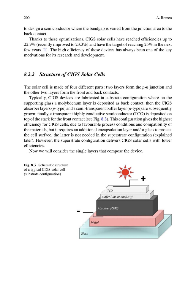
Typically, CIGS devices are fabricated in substrate configuration where on the
supporting glass a molybdenum layer is deposited as back contact, then the CIGS
absorber layers (p-type) and a semi-transparent buffer layer (n-type) are subsequently
grown; finally, a transparent highly conductive semiconductor (TCO) is deposited on
top of the stack for the front contact (see Fig. 8.3). This configuration gives the highest
efficiency for CIGS cells, due to favourable process conditions and compatibility of
the materials, but it requires an additional encapsulation layer and/or glass to protect
the cell surface, the latter is not needed in the superstrate configuration (explained
later). However, the superstrate configuration delivers CIGS solar cells with lower
efficiencies.
Now we will consider the single layers that compose the device.
Fig. 8.3 Schematic structure
of a typical CIGS solar cell
(substrate configuration)
A. Romeo
to design a semiconductor where the bandgap is varied from the junction area to the
back contact.
Thanks to these optimizations, CIGS solar cells have reached efficiencies up to
22.9% (recently improved to 23.3%) and have the target of reaching 25% in the next
few years [1]. The high efficiency of these devices has always been one of the key
motivations for its research and development.
8.2.2 Structure of CIGS Solar Cells
The solar cell is made of four different parts: two layers form the p-n junction and
the other two layers form the front and back contacts.
Typically, CIGS devices are fabricated in substrate configuration where on the
supporting glass a molybdenum layer is deposited as back contact, then the CIGS
absorber layers (p-type) and a semi-transparent buffer layer (n-type) are subsequently
grown; finally, a transparent highly conductive semiconductor (TCO) is deposited on
top of the stack for the front contact (see Fig. 8.3). This configuration gives the highest
efficiency for CIGS cells, due to favourable process conditions and compatibility of
the materials, but it requires an additional encapsulation layer and/or glass to protect
the cell surface, the latter is not needed in the superstrate configuration (explained
later). However, the superstrate configuration delivers CIGS solar cells with lower
efficiencies.
Now we will consider the single layers that compose the device.
Fig. 8.3 Schematic structure
of a typical CIGS solar cell
(substrate configuration)