

198
A. Romeo
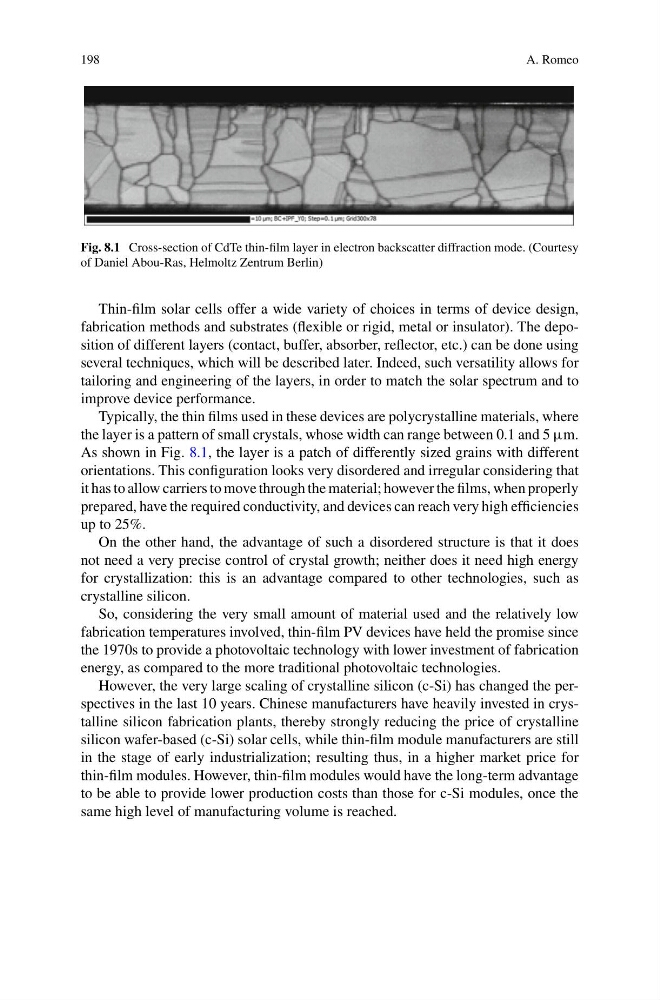
Fig. 8.1 Cross-section of CdTe thin-film layer in electron backscatter diffraction mode. (Courtesy
of Daniel Abou-Ras, Helmoltz Zentrum Berlin)
Thin-film solar cells offer a wide variety of choices in terms of device design,
fabrication methods and substrates (flexible or rigid, metal or insulator). The deposition of different layers (contact, buffer, absorber, reflector, etc.) can be done using
several techniques, which will be described later. Indeed, such versatility allows for
tailoring and engineering of the layers, in order to match the solar spectrum and to
improve device performance.
Typically, the thin films used in these devices are polycrystalline materials, where
the layer is a pattern of small crystals, whose width can range between 0.1 and 5 µm.
As shown in Fig. 8.1, the layer is a patch of differently sized grains with different
orientations. This configuration looks very disordered and irregular considering that
it has to allow carriers to move through the material; however the films, when properly
prepared, have the required conductivity, and devices can reach very high efficiencies
up to 25%.
On the other hand, the advantage of such a disordered structure is that it does
not need a very precise control of crystal growth; neither does it need high energy
for crystallization: this is an advantage compared to other technologies, such as
crystalline silicon.
So, considering the very small amount of material used and the relatively low
fabrication temperatures involved, thin-film PV devices have held the promise since
the 1970s to provide a photovoltaic technology with lower investment of fabrication
energy, as compared to the more traditional photovoltaic technologies.
However, the very large scaling of crystalline silicon (c-Si) has changed the perspectives in the last 10 years. Chinese manufacturers have heavily invested in crystalline silicon fabrication plants, thereby strongly reducing the price of crystalline
silicon wafer-based (c-Si) solar cells, while thin-film module manufacturers are still
in the stage of early industrialization; resulting thus, in a higher market price for
thin-film modules. However, thin-film modules would have the long-term advantage
to be able to provide lower production costs than those for c-Si modules, once the
same high level of manufacturing volume is reached.
A. Romeo
Fig. 8.1 Cross-section of CdTe thin-film layer in electron backscatter diffraction mode. (Courtesy
of Daniel Abou-Ras, Helmoltz Zentrum Berlin)
Thin-film solar cells offer a wide variety of choices in terms of device design,
fabrication methods and substrates (flexible or rigid, metal or insulator). The deposition of different layers (contact, buffer, absorber, reflector, etc.) can be done using
several techniques, which will be described later. Indeed, such versatility allows for
tailoring and engineering of the layers, in order to match the solar spectrum and to
improve device performance.
Typically, the thin films used in these devices are polycrystalline materials, where
the layer is a pattern of small crystals, whose width can range between 0.1 and 5 µm.
As shown in Fig. 8.1, the layer is a patch of differently sized grains with different
orientations. This configuration looks very disordered and irregular considering that
it has to allow carriers to move through the material; however the films, when properly
prepared, have the required conductivity, and devices can reach very high efficiencies
up to 25%.
On the other hand, the advantage of such a disordered structure is that it does
not need a very precise control of crystal growth; neither does it need high energy
for crystallization: this is an advantage compared to other technologies, such as
crystalline silicon.
So, considering the very small amount of material used and the relatively low
fabrication temperatures involved, thin-film PV devices have held the promise since
the 1970s to provide a photovoltaic technology with lower investment of fabrication
energy, as compared to the more traditional photovoltaic technologies.
However, the very large scaling of crystalline silicon (c-Si) has changed the perspectives in the last 10 years. Chinese manufacturers have heavily invested in crystalline silicon fabrication plants, thereby strongly reducing the price of crystalline
silicon wafer-based (c-Si) solar cells, while thin-film module manufacturers are still
in the stage of early industrialization; resulting thus, in a higher market price for
thin-film modules. However, thin-film modules would have the long-term advantage
to be able to provide lower production costs than those for c-Si modules, once the
same high level of manufacturing volume is reached.