

178
S. Leu and D. Sontag
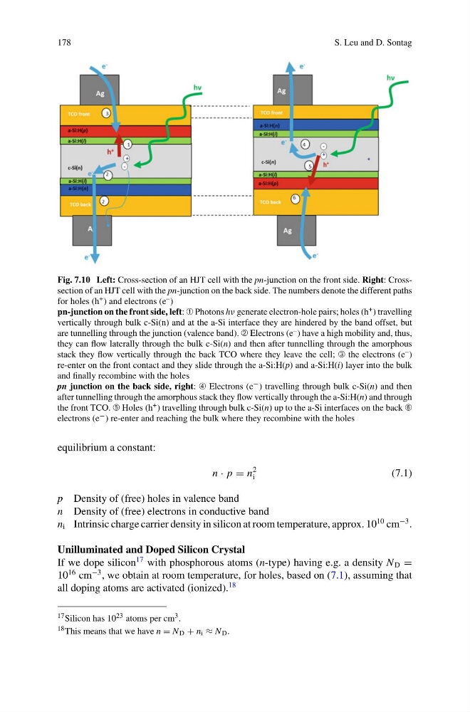
Fig. 7.10 Left: Cross-section of an HJT cell with the pn-junction on the front side. Right: Crosssection of an HJT cell with the pn-junction on the back side. The numbers denote the different paths
for holes (h + ) and electrons (e – )
pn-junction on the front side, left: ➀ Photons hν generate electron-hole pairs; holes (h + ) travelling
vertically through bulk c-Si(n) and at the a-Si interface they are hindered by the band offset, but
are tunnelling through the junction (valence band). ➁ Electrons (e – ) have a high mobility and, thus,
they can flow laterally through the bulk c-Si(n) and then after tunnelling through the amorphous
stack they flow vertically through the back TCO where they leave the cell; ➂ the electrons (e – )
re-enter on the front contact and they slide through the a-Si:H(p) and a-Si:H(i) layer into the bulk
and finally recombine with the holes
pn junction on the back side, right: ➃ Electrons (e − ) travelling through bulk c-Si(n) and then
after tunnelling through the amorphous stack they flow vertically through the a-Si:H(n) and through
the front TCO. ➄ Holes (h + ) travelling through bulk c-Si(n) up to the a-Si interfaces on the back ➅
electrons (e − ) re-enter and reaching the bulk where they recombine with the holes
equilibrium a constant:
n · p = n
2
i
(7.1)
p Density of (free) holes in valence band
n Density of (free) electrons in conductive band
n i Intrinsic charge carrier density in silicon at room temperature, approx. 10
10 cm
−3 .
Unilluminated and Doped Silicon Crystal
If we dope silicon
17 with phosphorous atoms (n-type) having e.g. a density N D =
10
16 cm
−3 , we obtain at room temperature, for holes, based on (7.1), assuming that
all doping atoms are activated (ionized).
18
17 Silicon has 10 23 atoms per cm 3 .
18 This means that we have n = N D + n i ≈ N D .
S. Leu and D. Sontag
Fig. 7.10 Left: Cross-section of an HJT cell with the pn-junction on the front side. Right: Crosssection of an HJT cell with the pn-junction on the back side. The numbers denote the different paths
for holes (h + ) and electrons (e – )
pn-junction on the front side, left: ➀ Photons hν generate electron-hole pairs; holes (h + ) travelling
vertically through bulk c-Si(n) and at the a-Si interface they are hindered by the band offset, but
are tunnelling through the junction (valence band). ➁ Electrons (e – ) have a high mobility and, thus,
they can flow laterally through the bulk c-Si(n) and then after tunnelling through the amorphous
stack they flow vertically through the back TCO where they leave the cell; ➂ the electrons (e – )
re-enter on the front contact and they slide through the a-Si:H(p) and a-Si:H(i) layer into the bulk
and finally recombine with the holes
pn junction on the back side, right: ➃ Electrons (e − ) travelling through bulk c-Si(n) and then
after tunnelling through the amorphous stack they flow vertically through the a-Si:H(n) and through
the front TCO. ➄ Holes (h + ) travelling through bulk c-Si(n) up to the a-Si interfaces on the back ➅
electrons (e − ) re-enter and reaching the bulk where they recombine with the holes
equilibrium a constant:
n · p = n
2
i
(7.1)
p Density of (free) holes in valence band
n Density of (free) electrons in conductive band
n i Intrinsic charge carrier density in silicon at room temperature, approx. 10
10 cm
−3 .
Unilluminated and Doped Silicon Crystal
If we dope silicon
17 with phosphorous atoms (n-type) having e.g. a density N D =
10
16 cm
−3 , we obtain at room temperature, for holes, based on (7.1), assuming that
all doping atoms are activated (ionized).
18
17 Silicon has 10 23 atoms per cm 3 .
18 This means that we have n = N D + n i ≈ N D .